Skip to the content
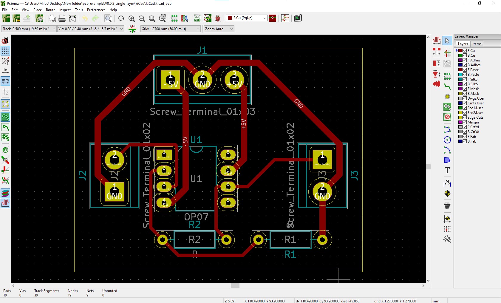
2 layers45.7 × 35.6 mmV0.0.2 single layer, the printed circuit board in 3D

V0.0.2 single layer

milos-nikolic/pcb-example

Reference example for printed board.

Size
45.7 × 35.6 mm
Copper layers
2
Thickness
1.6 mm
Parts
6
Nets
9
Pads
19
Tracks, vias
39, 0
Routed
Yes
KiCad
KiCad 5 (file 20171130)
Created
27 Jul 2020
Updated
5 Aug 2020

Overview

V0.0.2 single layer is an open-source printed circuit board by milos-nikolic, from the milos-nikolic/pcb-example repository on GitHub. It is a 2-layer board of 45.7 × 35.6 mm with 6 parts on 9 nets, routed with 39 tracks and 0 vias.

It is built around the OP07. Its parts include 3 connectors, 2 resistors and 1 IC.

Main components

1

README

README.md

This is basic pcb design example

With dual-layer

With dual-layer

With single-layer

With single-layer

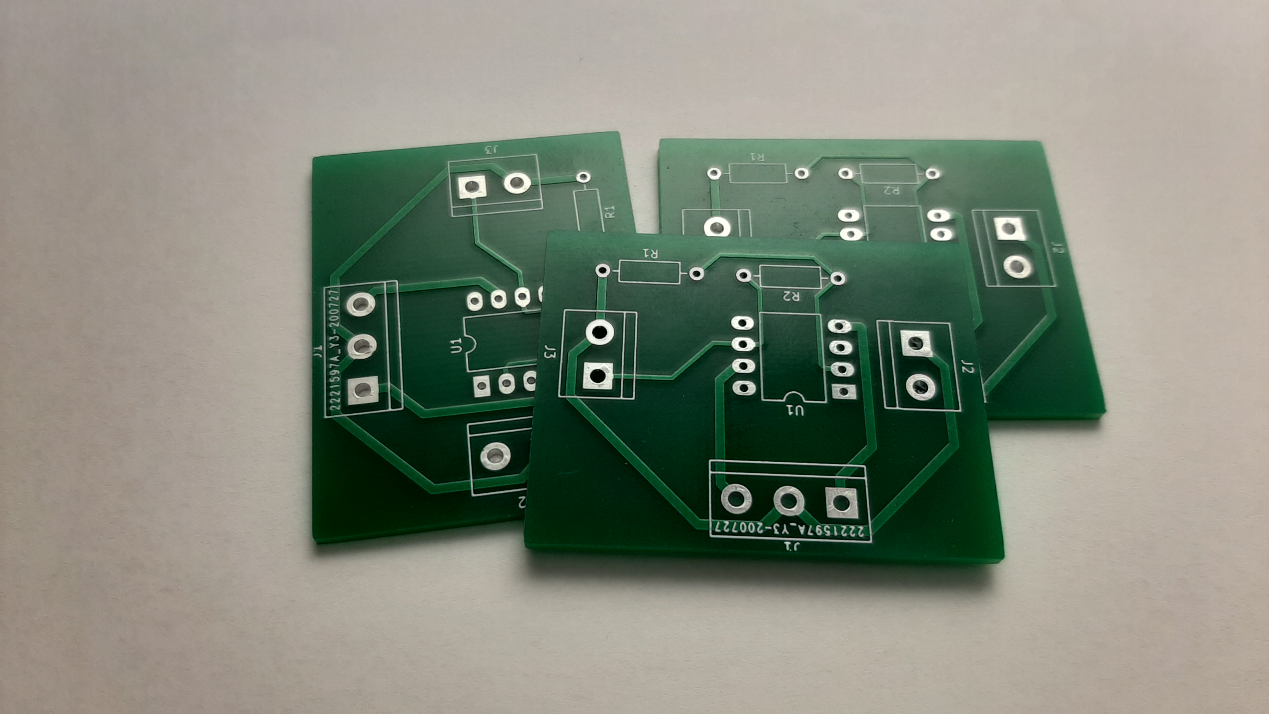
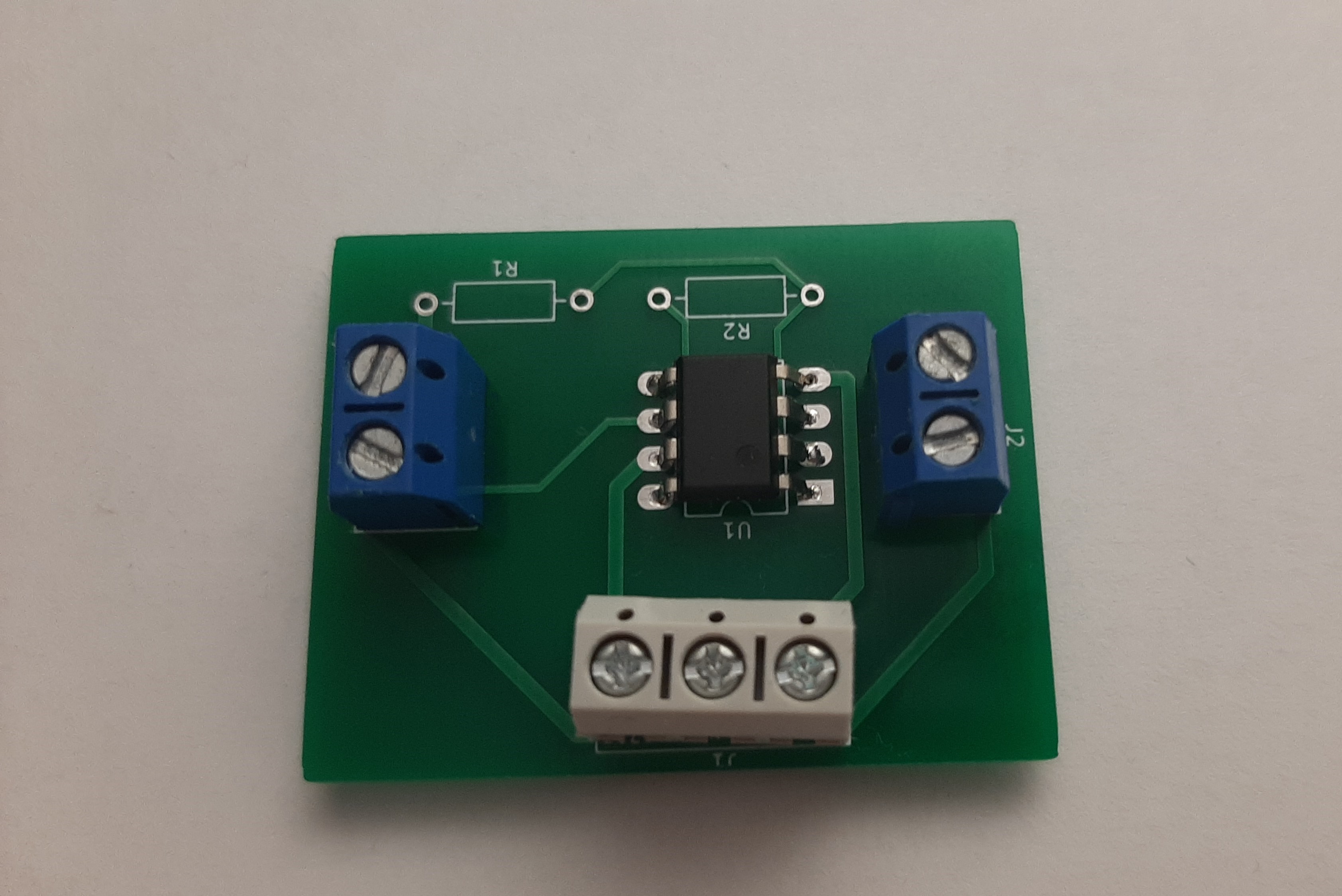
Produced ( ordered boards )

Produced

Populated

Produced

Parts

6
QtyValueFootprintReferences
2RResistor_THT:R_Axial_DIN0207_L6.3mm_D2.5mm_P10.16mm_HorizontalR1, R2
2Screw_Terminal_01x02TerminalBlock:TerminalBlock_bornier-2_P5.08mmJ2, J3
1OP07Package_DIP:DIP-8_W10.16mm_LongPadsU1
1Screw_Terminal_01x03TerminalBlock:TerminalBlock_bornier-3_P5.08mmJ1

Similar boards

  • 2 layers130 × 80 mmSmu main 1, the printed circuit board in 3D

    Smu main 1

    jaromir-sukuba/J-SMU

    DIY source-measure unit

    210 parts244
  • 2 layers118 × 103.5 mmEV Charger2, the printed circuit board in 3D

    EV Charger2

    fotherja/EV_Charger

    Arduino Uno Code for EV Charger

    62 parts167MIT
  • 2 layers144.8 × 88.9 mmPotentiostat, the printed circuit board in 3D

    Potentiostat

    iorodeo/potentiostat

    Rodeostat design files, software and firmware

    142 parts57CC-BY-4.0
  • 2 layers256 × 121 mmForte PA Deck, the printed circuit board in 3D

    Forte PA Deck

    SP6GK/Forte-600-HF-RF-Amplifier

    Project of 600 W LDMOS amlifier based on 2xMRF300.

    170 parts17GPL-3.0
  • 2 layers71 × 51 mmLetitrain, the printed circuit board in 3D

    Letitrain

    bseibold/letitrain

    An ESP32 board intended for use with TL-136 level sensors

    47 parts5MIT
  • 2 layers245.6 × 85.9 mmMycelium pcb, the printed circuit board in 3D

    Mycelium pcb

    microresearch/mycelium

    134 parts5GPL-3.0
  • 2 layers114 × 95 mmVCU V3.2, the printed circuit board in 3D

    VCU V3.2

    HKUST-Red-Bird-Racing-EVRT/GEN5_ELEC

    Repository for RBR EVRT 2025 EE

    170 parts3
  • 4 layers70 × 70.5 mmPCB FINAL UPDATED, the printed circuit board in 3D

    PCB FINAL UPDATED

    bash227/ECG-Motor-Control-Power-Management-PCB

    A multi-function PCB integrating biomedical signal acquisition (ECG), DC motor control, and advanced power management for wearable applications.

    111 parts2MIT

Questions

How big is the V0.0.2 single layer PCB?

It measures 45.7 × 35.6 mm and has 2 copper layers, 1.6 mm thick.

What parts does the V0.0.2 single layer use?

6 parts, built around the OP07. The full list of its parts is on this page, with links to each part's symbol and footprint where PCBKit's library has them.

Where can I download the V0.0.2 single layer KiCad files?

From the milos-nikolic/pcb-example repository on GitHub, at the commit this page was made from: the board is V0.0.2_single_layer/kiCad/kiCad.kicad_pcb. PCBKit opens the board in the browser, with nothing to install.

Can I use the V0.0.2 single layer design in my own project?

Its repository states no licence, so its author keeps all rights: ask milos-nikolic before reusing the design.