4 layers180 × 100 mm
Class board V0.2
TIGP-Experimental-Methods/class-board-2026
TIGP class instrument 2026: one board, five blocks - KiCad hardware, ESP32-S3 firmware, phone PWA, Python API, workbook
342 parts

 maximevince/PicoZorro2
Amiga Zorro-II Bus Cards using nothing but an RPi Pico to interact with the bus
Picozorro one th is an open-source printed circuit board by maximevince, from the maximevince/PicoZorro repository on GitHub. It is a 2-layer board of 155.5 × 65.9 mm with 48 parts on 125 nets, routed with 546 tracks and 286 vias.
It is built around the AMS1117-3.3, LD1117V33 and CL31A226KAHNNNE, with the CC0603KRX7R9BB104, CL21A106KAYNNNE and MMBT3904 among its other parts. Its parts include 16 capacitors, 10 connectors, 7 resistors, 2 ICs and 2 diodes.


The PicoZorro One is the Zorro II network and USB card of the PicoZorro project. The One TH is its through-hole version: bought modules and a handful of through-hole parts on a bare two-layer PCB. Every through-hole part also has an SMD alternate on the same board, so the same PCB can be assembled by JLCPCB instead (see "Two builds" below).
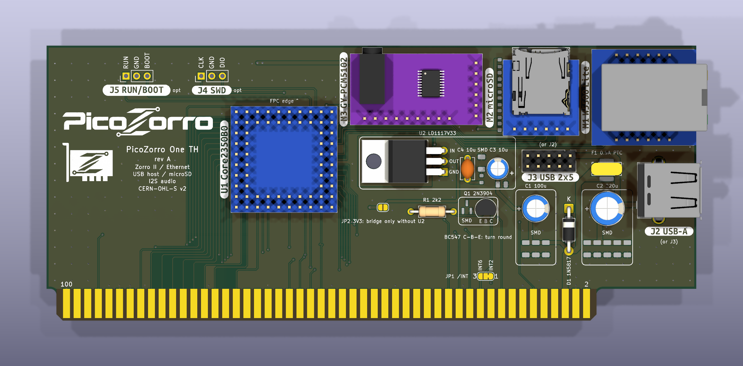
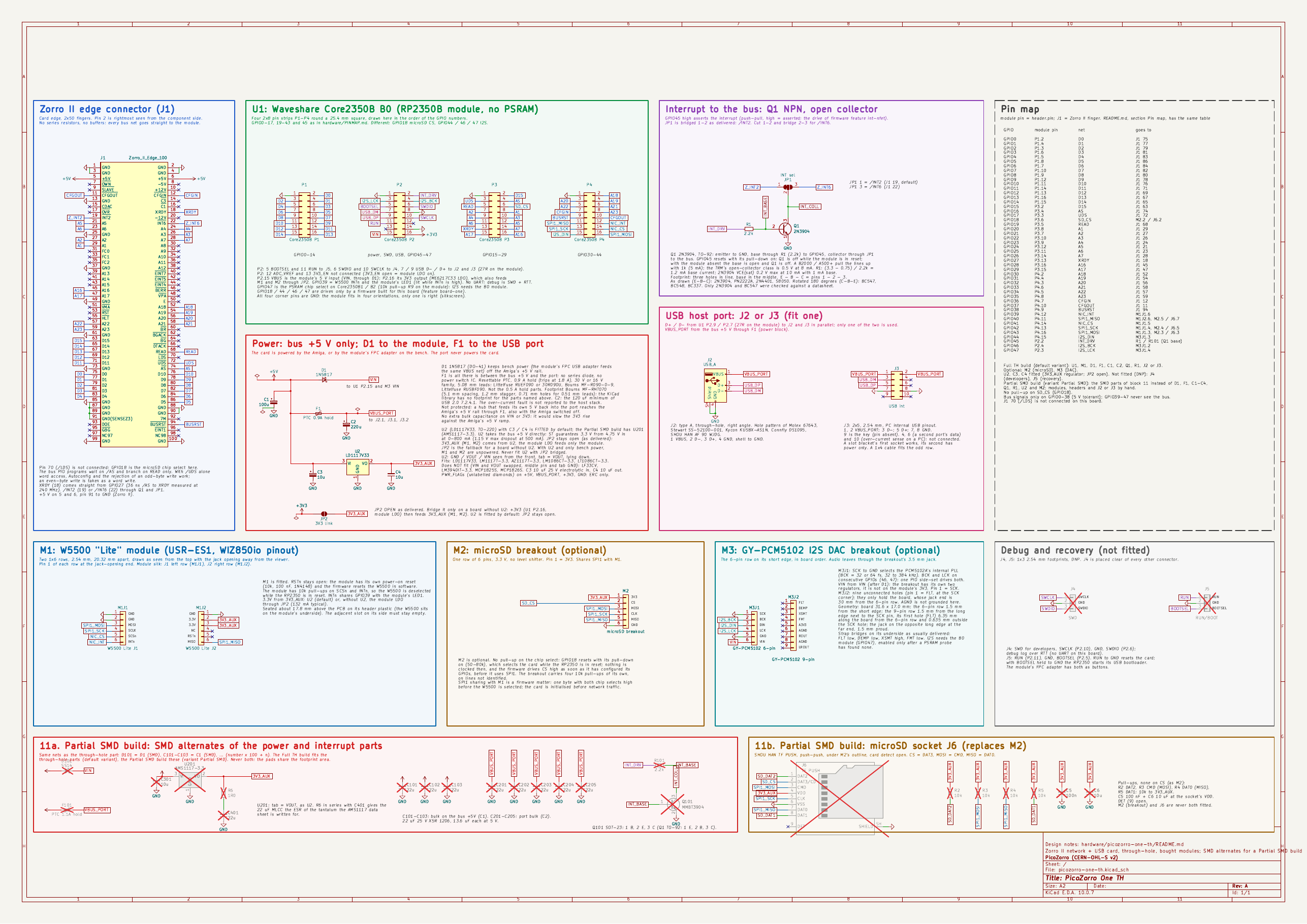
Rev A. The schematic and the routed board pass KiCad ERC and DRC with zero
violations, DRC with schematic parity (make check-one-th at the top of the
repository). Rev A boards of the Partial SMD build are built and run in an
Amiga: network, USB host and the microSD block device. The DAC does not
play yet, and the Full TH build has not been built. The open points are
listed at the end of this file.
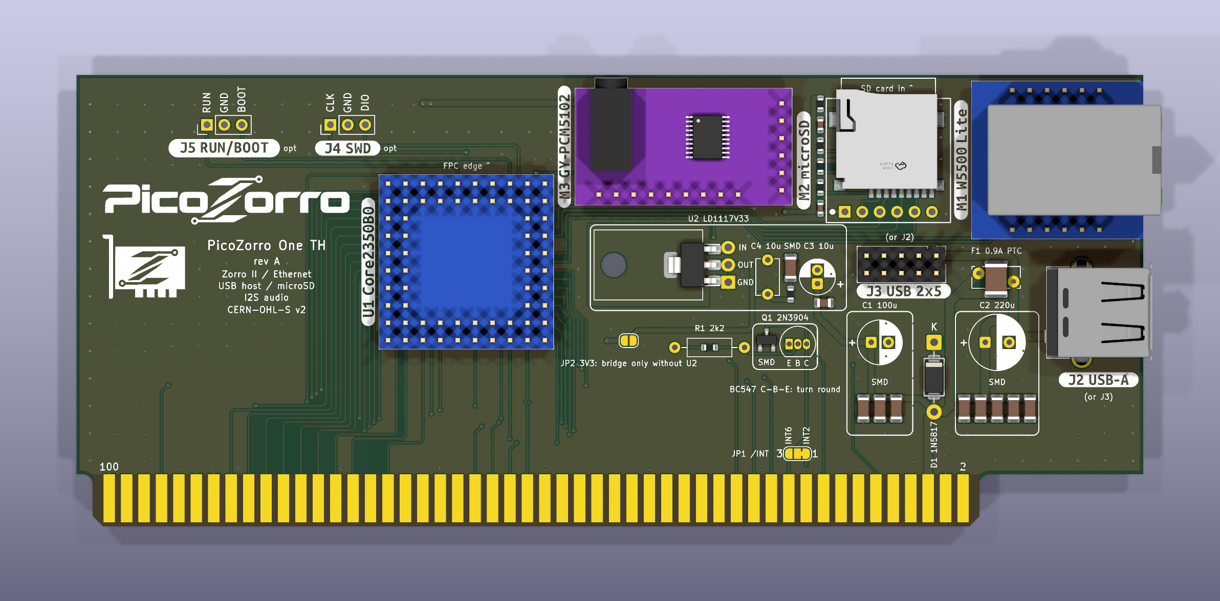
One PCB, two builds. The Full TH build (KiCad's default variant) fits
every part through-hole, soldered by hand. The Partial SMD build (KiCad
variant Partial SMD) has JLCPCB place an SMD set, almost all JLC Basic
parts, and optionally solder the USB-A socket J2; the builder then solders
only the modules on their headers (and J2 or J3 if JLC did not).
Each through-hole part and its SMD alternate sit on the same nets and share the footprint area; the two are never both fitted. The SMD alternate of a part has the part's number times 100 plus 1, 2, ... as its reference (D101 is D1's, C101-C103 are C1's bank), because KiCad cannot give one symbol two footprints. The board hides those references; silk frames group each pair under one label, and the JLC files name them "D1 (SMD)".
| Path | What |
|---|---|
picozorro-one-th.kicad_pro, .kicad_sch, .kicad_pcb, .kicad_dru | KiCad 10 project with the variant Partial SMD; the edge-connector and microSD socket footprints come from ../lib |
fab/gerbers/, fab/picozorro-one-th-gerbers.zip | Gerber and Excellon drill files, the same for both builds |
fab/picozorro-one-th-parts.csv | parts list of the Full TH build (the SMD alternates show DNP) |
fab/jlc/picozorro-one-th-bom-jlc.csv, fab/jlc/picozorro-one-th-cpl-jlc.csv | JLC BOM (the SMD set with LCSC numbers; the through-hole alternates as DNP) and placement file (SMD set and J2, rotations corrected for JLC) |
fab/order-notes.txt | the options to pick in the order form, and what the builder solders in each build |
3d/ | STEP models of the modules and the PTC that the board references; origins and licences in 3d/SOURCES.txt |
images/ | schematic (PDF, PNG), copper and silkscreen views, 3D renders: pcb-3d-th.png (Full TH build), pcb-3d-jlc.png (Partial SMD build, same view), pcb-3d-iso.png (Full TH build, isometric) |
Full TH build, everything by hand. The last column names the SMD alternate the Partial SMD build fits instead (LCSC part number in brackets; JLC Basic parts unless marked Extended).
| Ref | Part | Value / type | Package | Fitted (Full TH) | Partial SMD build alternate |
|---|---|---|---|---|---|
| U1 (P1-P4) | Waveshare Core2350B0 module (no PSRAM) | - | four 2x8 2.54 mm pin strips | yes | same, by hand |
| M1 | W5500 "Lite" module (USR-ES1, WIZ850io pinout) | - | two 1x6 2.54 mm rows | yes | same, by hand |
| M2 | microSD breakout, 3.3 V, no level shifter | - | one 1x6 2.54 mm row | optional | J6, SHOU HAN TF PUSH push-push socket (C393941, Extended), with R2-R5 and C5, C6 |
| M3 | PCM5102A DAC breakout "GY-PCM5102" | - | 1x6 row (signals) + 1x9 row (holding only) | optional | same, by hand (optional) |
| D1 | Schottky diode | 1N5817 | DO-41, 10.16 mm | yes | D101, SS14, SMA (C2480) |
| F1 | resettable PTC fuse, 30 V (or 16 V) family | 0.9 A hold, e.g. Littelfuse RUEF090 | radial, 5.08 mm leads | yes | F101, 1.1 A hold, 1812, Brightking SMD1812B110TF/33 (C269134, Extended) |
| C1 | electrolytic capacitor, bus +5 V | 100 uF | radial, D6.3 mm, 2.5 mm pitch | yes | C101-C103, 3 x 22 uF 25 V X5R 1206 (C12891) |
| C2 | electrolytic capacitor, USB port | 220 uF | radial, D8 mm, 3.5 mm pitch | yes | C201-C205, 5 x 22 uF 25 V X5R 1206 (C12891) |
| U2 | 3.3 V regulator for 3V3_AUX | LD1117V33 | TO-220, lying down | yes | U201, AMS1117-3.3, SOT-223, tab = VOUT (C6186) |
| C3 | U2 input capacitor | 10 uF 25 V electrolytic | radial, D5 mm, 2 mm pitch | yes | C301, 10 uF 25 V X5R 0805 (C15850) |
| C4 | U2 output capacitor | 10 uF | disc, 5 mm pitch | yes | R6 1.0 ohm 0603 (C22936) in series with C401 22 uF 1206 (C12891) |
| Q1 | NPN transistor | 2N3904 | TO-92, E-B-C | yes | Q101, MMBT3904, SOT-23, 1 B / 2 E / 3 C (C20526) |
| R1 | resistor, GPIO45 to Q1 base | 2.2 k | axial, DIN0207, 10.16 mm | yes | R101, 2.2 k 0603 (C4190) |
| J2 | USB 2.0 type A receptacle, right angle | Molex 67643 pattern | through-hole | one of J2 / J3 | SHOU HAN AF 90 WJDG (C456018), soldered by JLC, optional at order time |
| J3 | PC internal USB header | 2x5, pin 9 absent | 2.54 mm header | one of J2 / J3 | same, by hand |
| J4 | SWD header: SWCLK / GND / SWDIO | - | 1x3 2.54 mm | no (developers) | same |
| J5 | recovery header: RUN / GND / BOOTSEL | - | 1x3 2.54 mm | no (recovery) | same |
The Partial SMD build adds, with J6 only: R2-R5, 10 k 0603 pull-ups on DAT2, CMD (MOSI), DAT0 (MISO) and DAT1 (C25804); C5 100 nF 0603 (C14663) and C6 10 uF 0603 (C96446) at J6's VDD.
U1 must be the B0 variant in both builds: on the B1 / B2 modules GPIO47 is the PSRAM chip select, and this board needs GPIO47 for the I2S word clock. The microSD chip select (GPIO18) works on any variant.
The parts lists are fab/picozorro-one-th-parts.csv (Full TH)
and fab/jlc/picozorro-one-th-bom-jlc.csv (Partial SMD).
F1 alternatives: Littelfuse RUEF090 or 30R090U, Bourns MF-R090-0-9,
Littelfuse RUSBF090 (0.07-0.12 ohm new, 0.22 ohm at most after a trip;
holds 0.57-0.61 A at 60 C). Not the 0.5 A hold parts: they hold 0.36 A at
50 C and drop up to 0.59 V. The footprint is KiCad's
Fuse_Bourns_MF-RHT070 (5.1 mm lead spacing with the 1.2 mm stagger of a
radial PTC's leads, 0.71 mm holes for 0.51 mm leads); the KiCad library
has no footprint for the parts named above.
Q1 alternatives: the footprint is three holes in line, base in the middle, emitter - base - collector as pins 1-2-3.
| Part | Pin order 1-2-3 | Fits |
|---|---|---|
| 2N3904, PN2222A, 2N4401, S8050 | E-B-C | as drawn |
| BC547, BC548, BC337 | C-B-E | rotated 180 degrees (silkscreen: "BC547 C-B-E: turn round") |
Only the 2N3904 and the BC547 were checked against a data sheet; check the others before fitting.
U2 alternatives (pin order GND / VOUT / VIN seen from the front, tab = VOUT): LD1117V33, LM1117T-3.3, AZ1117T-3.3, LM1086CT-3.3, LT1086CT-3.3. They do not fit with VIN and VOUT swapped, middle pin GND, tab GND: LF33CV, LM3940IT-3.3, MCP1825S, MCP1826S. The silkscreen names the three holes. C3 is an electrolytic: mind its polarity.
| Jumper | As delivered | Change |
|---|---|---|
| JP1 | bridged 1-2 by a trace: Q1 collector to /INT2 (J1 pin 19) | cut 1-2 and bridge 2-3 for /INT6 (J1 pin 22) |
| JP2 | open in both builds: U2 (Full TH) or U201 (Partial SMD) supplies 3V3_AUX | fallback for a board without U2: bridge it, and the module's 3V3 (U1 P2.16) feeds 3V3_AUX. Never bridge it with U2 or U201 fitted |
The PicoZorro GPIO map (../PINMAP.md) applies to GPIO0-17, 19-43 and 45.
Four pins differ on this board:
| GPIO | Module pin | Shared map | This board |
|---|---|---|---|
| 18 | P3.6 | /LDS | microSD chip select |
| 44 | P4.15 | /ARM | I2S data (DIN) |
| 46 | P2.4 | UART0 TX | I2S bit clock (BCK) |
| 47 | P2.3 | not connected / PSRAM chip select | I2S word clock (LCK), B0 module only |
The whole map:
| GPIO | Signal | Goes to |
|---|---|---|
| 0-15 | D0-D15 | J1 |
| 16 | /AS | J1 74 |
| 17 | /UDS | J1 72 |
| 18 | SD_CS | M2 pin 2 / J6 DAT3 |
| 19 | READ | J1 68 |
| 20-26 | A1-A7 | J1 |
| 27 | XRDY | J1 18, direct |
| 28-35 | A16-A23 | J1 |
| 36 | /CFGIN | J1 12 |
| 37 | /CFGOUT | J1 11 |
| 38 | /BUSRST | J1 94 |
| 39 | NIC_INT | M1 INTn (the module's LED1 is on the same pin, lit while INTn is high) |
| 40 | SPI1 MISO | M1, M2 / J6 DAT0 |
| 41 | NIC_CS | M1 SCSn |
| 42 | SPI1 SCK | M1, M2 / J6 CLK |
| 43 | SPI1 MOSI | M1, M2 / J6 CMD |
| 44 | I2S_DIN | M3 |
| 45 | INT_DRV | R1 / R101, Q1 / Q101 base |
| 46 | I2S_BCK | M3 |
| 47 | I2S_LCK | M3 |
Bus signals use only GPIO0-38 (5 V tolerant); GPIO39-47 never see the bus. The bus nets go straight from the edge fingers to the module pins: no series resistors, no buffers. XRDY comes from GPIO27 directly (36 ns from /AS to XRDY measured at 240 MHz). The edge connector (J1) has +5 V on pins 5 and 6, all GND pins connected and pin 91 tied to GND.
There is no UART: debug is SWD with RTT on J4.
/LDS (J1 pin 70) is not connected. The bus PIO programs wait on /AS and branch on READ only; the strobes are two bits of the sampled word, used by the register model to tell word from byte access. With /UDS alone, word access, Autoconfig (its writes are /UDS-only bytes on D15-D8) and the rejection of an odd-byte write (/UDS high) work; an even-byte write cannot be told from a word write and is taken as a word write.
GPIO47 and the module variant. On the Core2350B B1 / B2 modules the PSRAM chip select sits directly on GPIO47 with a 10 k pull-up (R9); R11 (0 R) only links the net to header pin P2.3. Driving GPIO47 there selects the PSRAM during flash access. I2S therefore needs the B0 module, and the firmware must not drive GPIO47 unless a PSRAM probe has found none.
This board's image is the default firmware build plus the feature
board-one (make fw-uf2 FEATURES=board-one at the top of the repository).
The defaults xrdy-direct (GPIO27 pulls XRDY) and int-nfet (GPIO45
push-pull, high asserts /INT) match the bus side; board-one drives GPIO18
high from boot as the microSD chip select, leaves GPIO44 / 46 / 47 to the
DAC and has no UART log. A default build without it drives GPIO44 as /ARM and
GPIO46 as the UART log. make fw-one builds a bring-up image with the USB
CDC log and bench commands (W5500 version, microSD init, /INT toggle, a DAC
test tone).
board-one brings the microSD block device (feature sd; registers in
docs/REGISTERS.md, "microSD block device"):
The I2S driver is not written yet; I2S is enabled only after a PSRAM probe has found none.
J1 +5V --+-- C1 --GND
         |
         +-- D1 -->|-- VIN ---- U1 P2.15 (VBUS: module LDO input)
         |                 +--- M3 VIN
         |
         +-- F1 ---+--- VBUS_PORT --- J2.1, J3.1, J3.2
         |         +--- C2 --GND
         |
         +-- C3 --- U2 --- C4 --- 3V3_AUX --- M1, M2 / J6

U1 P2.16 (3V3, module LDO output) --- JP2 (open; bridged only without U2) --- 3V3_AUX
Partial SMD build: D101, F101 and U201 (C301 at its input, R6 + C401 at its output) in place of D1, F1 and U2 (C3, C4); the bulk is two MLCC banks, C101-C103 on the bus +5 V for C1 and C201-C205 on VBUS_PORT for C2 (40.9 and 68.2 uF effective at 5 V). JP2 stays open in both builds.
Port voltage from a 5.0 V rail at 500 mA: 5.0 - 0.06 (F1 new, 0.11 after a trip) = 4.94 V (4.89 V). USB 2.0 Table 7-7 asks for 4.75 V at a high-power port, so the rail may sag to 4.86 V. Section 7.2.1.2.1 asks for resettable over-current protection below 5.0 A: F1 trips at 1.8 A (Intel's guide sizes a single-port fuse at 1.5 A trip or more). The fault is not reported to the host stack: there is no pin for it.
USB 2.0 section 7.2.4.1 asks for no less than 120 uF of low-ESR capacitance on the downstream VBUS "per hub", to keep the power of the other ports within 330 mV when a device is plugged in (load model 10 uF with 44 ohm). This card has one port: the only other load on that VBUS is the card's own +5 V entry (D1 to VIN, U2) and, behind it, the Amiga rail. So both stay: C1 at the entry, C2 at the port, F1 between them (on a microsecond scale the PTC is a plain resistor that isolates the two).
A hot-plug simulation (1 m cable, assumed rail and ESR values, not a measurement) puts the entry droop at 0.23 / 0.15 V (PTC 0.1 / 0.3 ohm) with the Partial SMD build's ceramic banks, the smallest of the arrangements tried at 0.3 ohm, matched only by a low-ESR polymer 220 uF at the entry (0.22 / 0.17 V). The Full TH build's two electrolytics give 0.43 / 0.29 V; a single ordinary electrolytic at the entry (0.15 ohm ESR) 0.61 / 0.45 V, worse than either split. The port itself dips 0.4 to 3 V for microseconds whatever is fitted: no arrangement holds it within 330 mV with a stick plugged straight in. Both builds lay the two groups out alike: the electrolytic on top, its MLCC row under it in the 15 mm band.
3V3_AUX (M1, M2 / J6) has its own regulator, U2, fitted in both builds; JP2 stays open and the module's LDO feeds only the module. The loads: M1 132 mA typical (W5500 data sheet section 5.4; the WIZ850io module 141 mA), M2 up to 100 mA, the maximum averaged over 1 s in SPI mode (SD Physical Layer Simplified Specification v3.01, Table 3-4 note 7; SanDisk's manual gives 65 mA read and 75 mA write at most). The simplified specification gives no peak or inrush figure. That is about 0.22 A typical, 0.24-0.27 A at those ceilings. M3 is not on this rail: its VIN comes from VIN and it has its own two regulators.
U2 takes the bus +5 V directly, not behind D1. Full TH build: LD1117V33. ST guarantees 3.235-3.365 V out for Vin 4.75-10 V at 0-800 mA (TJ 0-125 C, LD1117 data sheet DocID2572 Rev 38, Table 6), dropout 1.15 V at most at 500 mA: it regulates from 4.45 V, a 0.30 V margin at the bus's 4.75 V minimum. The Partial SMD build fits U201, an AMS1117-3.3 (SOT-223, the same pin order, tab = VOUT) under U2's footprint, its tab on the same 3V3_AUX copper area. Its only guaranteed dropout is 1.3 V at 800 mA, so it needs 4.60 V: a margin of about 0.15 V. R6 (1.0 ohm) in series with C401 (22 uF) at its output gives the ceramic the ESR of the tantalum the AMS1117 data sheet is written for. Dissipation in either build: (5.25 V - 3.3 V) x 0.3 A = 0.59 W at most.
The module's regulator is the fallback (JP2 bridged on a board without U2), not the default: the ME6217C33M5G data sheet gives 800 mA as a typical IOUT(max) (and as the absolute maximum), no minimum, and notes it may not be reached because of package dissipation; it gives no thermal resistance. Its sibling ME6207 rates the SOT-23-5 package at 250 mW. The W5500 alone puts 0.25-0.41 W into it, with an SD card 0.45-0.66 W. Measured with a thermal camera, module plus W5500 on the module's 3V3, room 20 C: nothing on the module above 40 C (no SD card in that measurement).
There is no extra bulk capacitance on VIN or 3V3: it would slow the 3V3 rise against the Amiga's +5 V ramp.
Q1, an NPN transistor, drives the interrupt line open collector: emitter to GND, base through R1 (2.2 k) to GPIO45, collector through JP1 to /INT2 (default) or /INT6. GPIO45 high asserts the interrupt. GPIO45 resets with its pull-down on, so Q1 is off while the module is in reset; with the module absent the base is open and Q1 is off. GPIO45 is not 5 V tolerant, so it cannot pull the bus line itself.
Sizing: a B2000 and an A500+ pull both lines up with 1 k (5 mA at 5 V); the Technical Reference Manual's open-collector drive class is 0.5 V at 8 mA, so the driver must sink at least 8 mA. R1 gives (3.3 - 0.75) / 2.2 k = 1.2 mA of base current. The 2N3904 is specified at VCE(sat) 0.2 V maximum for 10 mA with 1 mA into the base, the BC547 at 0.25 V maximum (0.09 V typical) for 10 mA with 0.5 mA: both operating points are covered with margin.
A transistor and not a MOSFET: the through-hole MOSFETs hobby shops carry (2N7000, BS170) have gate thresholds up to 3 V and are not specified at 3.3 V drive; the one that is (TN0702) is a distributor-only part. Small NPN types are sold everywhere.
Simulated with ngspice (vendor models, 1 k to 10 k pull-ups, 4.75 to 5.25 V, 0 to 70 C, GPIO45 down to 3.0 V, R1 +5 %): /INT sits below 90 mV with a 2N3904 and below 40 mV with a BC547B, also at a forced 8 mA; GPIO45 sources 1.15 mA at most. Assertion takes under 125 ns into 1 nF. Release is the pull-up RC plus the transistor's storage time: 0.25 to 0.5 us for the 2N3904, 1.4 to 2.2 us for the BC547B, so 10 k with 500 pF reaches 2.0 V after 3.2 us (2N3904) or 4.9 us (BC547B). The 2N3904 is the default for that reason.
M1, W5500 Lite. Two 1x6 rows, 2.54 mm pitch, 20.32 mm apart; module 23.0 x 25.0 mm; pin 1 of each row at the jack-opening end, 6.4 mm from that edge; the jack overhangs that edge by 2.5-2.7 mm. Seen from the top with the jack opening away from the viewer (module silk J1 left, J2 right, jack HR961160C):
| Left row (J1) | Right row (J2) | ||
|---|---|---|---|
| 1 GND | GND | 1 GND | GND |
| 2 GND | GND | 2 3.3V | 3V3_AUX |
| 3 MOSI | GPIO43 | 3 3.3V | 3V3_AUX |
| 4 SCLK | GPIO42 | 4 NC | - |
| 5 SCSn | GPIO41 | 5 RSTn | not connected |
| 6 INTn | GPIO39 | 6 MISO | GPIO40 |
J1 pin 5 is SCSn as on the W5500 and the USR-ES1 schematic; WIZnet's WIZ850io page spells it SCNn.
RSTn stays open: the module has its own power-on reset (10 k, 100 nF, 1N4148) and the firmware resets the chip in software. The module has 10 k pull-ups on SCSn and INTn, so the W5500 is deselected while the RP2350 is in reset.
M2, microSD breakout. One 1x6 row: 3V3 (pin 1, to 3V3_AUX), CS (GPIO18), MOSI (GPIO43), CLK (GPIO42), MISO (GPIO40), GND. Board 18 x 18 mm (18.1 mm over its scored edges); the socket, 13.7 mm wide, overhangs the edge opposite the pin row by 3 mm and the card enters from there. No pull-up on the chip select: GPIO18 resets with its pull-down on (about 50-80 k), which selects the card while the RP2350 is in reset; nothing is clocked then, and the firmware drives the chip select high as soon as it has configured its GPIOs, before it uses SPI1. The breakout carries four 10 k pull-ups of its own, on lines not identified.
J6, microSD socket (Partial SMD build). A SHOU HAN TF PUSH push-push
socket (PicoZorro:microSD_ShouHan_TF-PUSH, ../lib/README.md) under M2's
outline, on M2's nets, the card entering over the top edge as with M2: CS =
DAT3 (GPIO18), MOSI = CMD, CLK, MISO = DAT0, VDD = 3V3_AUX. 10 k pull-ups R2
(DAT2), R3 (CMD / MOSI), R4 (DAT0 / MISO), R5 (DAT1), none on CS; C5 100 nF
and C6 10 uF at VDD. Card detect (pin 9) is not connected: no GPIO is free;
the firmware polls the card instead. M2 and J6 are never both fitted.
M3, GY-PCM5102. The 6-pin row on its short edge: SCK to GND (selects the PCM5102A's internal PLL), BCK to GPIO46, DIN to GPIO44, LCK to GPIO47, GND, VIN to VIN. Pin 1 is SCK. The 9-pin row (FLT, DEMP, XSMT, FMT, A3V3, AGND, ROUT, AGND, LROUT from the SCK corner) gets nine unconnected holes: it only holds the board. Audio leaves through the breakout's 3.5 mm jack. The four strap bridges on its underside stay as usually delivered: FLT low, DEMP low, XSMT high, FMT low. BCK and LCK are on consecutive GPIOs so one PIO side-set drives both; PLL mode accepts BCK = 32 fs or 64 fs from 32 kHz to 384 kHz. Geometry, from a third-party footprint (sstojos, zynthian-miniature) cross-checked against board photos: board 31.6 x 17.0 mm; the 6-pin row 1.5 mm from the short edge; the 9-pin row 1.5 mm from the long edge next to the SCK pin, its first hole (FLT) 6.35 mm along the board from the 6-pin row and 0.635 mm outside the SCK hole.
../EDGE_CONNECTOR.md. ENIG with a 0.5 x 45 degree bevel on the
finger edge is recommended; HASL works. The finger area is one open
solder-mask window by design. JLC's Economic PCBA offers no gold fingers:
ENIG without the bevel there, or Standard PCBA for hard-gold bevelled
fingers. The rev A boards so far were Economic PCBA with HASL and no
bevel, and they work in the slot; ENIG with a bevel is likely the better
choice for long-term use.| Target | Body height | Length | Slot pitch |
|---|---|---|---|
| Enterlogic A-NIC outline | 45.1 | 155.5 | - |
| Denise, low-profile PC card envelope | 58.3 max | about 168 | 15.24 |
| Denise, full-height PC card envelope | 100.6 max | about 171 over the board | 15.24 |
| A2000 and the Zorro II form factor | 114.5 max | 337.19 max | 20.32 |
On the Denise the card's shoulder rests 13.97 mm above the motherboard (EDAC 745-100-520-206, notched ends), and the card goes into the slot next to the CPU (CN4). Mini-ITX guarantees only 57 mm of free height over that slot, which is a 43.0 mm body; the One TH relies on the case for the rest.
../EDGE_CONNECTOR.md on the bare board (pins 2 and 4 are GND,
pin 6 is +5 V; they sit at the rear/bracket end). Then, with the strips
soldered and nothing else fitted, check for shorts between +5 V, 3V3
and GND.hello as a UF2 (make fw-uf2 BIN=hello at the top of the repository), hold BOOTSEL (J5, or the FPC
adapter's button) while the module powers up from its FPC adapter, and
copy firmware/hello.uf2 onto the USB drive that appears. Its USB CDC
log shows the chip's stepping and MAC. D1 keeps this bench power off
the bus pins.bus-listen the same way (make fw-uf2 BIN=bus-listen, firmware/bus-listen.uf2). It drives nothing on the
bus and prints the bus pins and the /AS statistics once a second on the
USB CDC log, so a wrong finger shows up before anything is driven.make fw-uf2 FEATURES=board-one, drop
firmware/picozorro-install.uf2 the same way (or make fw-install with
an SWD probe; docs/UPDATE.md), and pztest on the Amiga finds the
card and exercises its scratch register.int-nfet drive was run against a 2N7002 MOSFET, not an NPN transistor.| Qty | Value | Footprint | References |
|---|---|---|---|
| 9 | 22u | Capacitor_SMD:C_1206_3216Metric | C101, C102, C103, C201, C202, C203, C204, C205, C401 |
| 4 | 10k | Resistor_SMD:R_0603_1608Metric | R2, R3, R4, R5 |
| 1 | 100n | Capacitor_SMD:C_0603_1608Metric | C5 |
| 1 | 100u | Capacitor_THT:CP_Radial_D6.3mm_P2.50mm | C1 |
| 1 | 10u | Capacitor_THT:CP_Radial_D5.0mm_P2.00mm | C3 |
| 1 | 10u | Capacitor_SMD:C_0805_2012Metric | C301 |
| 1 | 10u | Capacitor_THT:C_Disc_D5.1mm_W3.2mm_P5.00mm | C4 |
| 1 | 10u | Capacitor_SMD:C_0603_1608Metric | C6 |
| 1 | 1N5817 | Diode_THT:D_DO-41_SOD81_P10.16mm_Horizontal | D1 |
| 1 | 1R0 | Resistor_SMD:R_0603_1608Metric | R6 |
| 1 | 2.2k | Resistor_THT:R_Axial_DIN0207_L6.3mm_D2.5mm_P10.16mm_Horizontal | R1 |
| 1 | 2.2k | Resistor_SMD:R_0603_1608Metric | R101 |
| 1 | 220u | Capacitor_THT:CP_Radial_D8.0mm_P3.50mm | C2 |
| 1 | 2N3904 | Package_TO_SOT_THT:TO-92_Inline | Q1 |
| 1 | 3V3 link | Jumper:SolderJumper-2_P1.3mm_Open_RoundedPad1.0x1.5mm | JP2 |
| 1 | AMS1117-3.3 | Package_TO_SOT_SMD:SOT-223-3_TabPin2 | U201 |
| 1 | Core2350B P1 | Connector_PinHeader_2.54mm:PinHeader_2x08_P2.54mm_Vertical | P1 |
| 1 | Core2350B P2 | Connector_PinHeader_2.54mm:PinHeader_2x08_P2.54mm_Vertical | P2 |
| 1 | Core2350B P3 | Connector_PinHeader_2.54mm:PinHeader_2x08_P2.54mm_Vertical | P3 |
| 1 | Core2350B P4 | Connector_PinHeader_2.54mm:PinHeader_2x08_P2.54mm_Vertical | P4 |
| 1 | GY-PCM5102 6-pin | Connector_PinHeader_2.54mm:PinHeader_1x06_P2.54mm_Vertical | M3J1 |
| 1 | GY-PCM5102 9-pin | Connector_PinHeader_2.54mm:PinHeader_1x09_P2.54mm_Vertical | M3J2 |
| 1 | INT sel | Jumper:SolderJumper-3_P1.3mm_Bridged12_RoundedPad1.0x1.5mm_NumberLabels | JP1 |
| 1 | LD1117V33 | Package_TO_SOT_THT:TO-220-3_Horizontal_TabDown | U2 |
| 1 | MMBT3904 | Package_TO_SOT_SMD:SOT-23 | Q101 |
| 1 | PTC 0.9A hold | Fuse:Fuse_Bourns_MF-RHT070 | F1 |
| 1 | PTC 1.1A hold | Fuse:Fuse_1812_4532Metric | F101 |
| 1 | RUN/BOOT | Connector_PinHeader_2.54mm:PinHeader_1x03_P2.54mm_Vertical | J5 |
| 1 | SS14 | Diode_SMD:D_SMA | D101 |
| 1 | SWD | Connector_PinHeader_2.54mm:PinHeader_1x03_P2.54mm_Vertical | J4 |
| 1 | TF PUSH | PicoZorro:microSD_ShouHan_TF-PUSH | J6 |
| 1 | USB int | Connector_PinHeader_2.54mm:PinHeader_2x05_P2.54mm_Vertical | J3 |
| 1 | USB_A | Connector_USB:USB_A_Molex_67643_Horizontal | J2 |
| 1 | W5500 Lite J1 | Connector_PinHeader_2.54mm:PinHeader_1x06_P2.54mm_Vertical | M1J1 |
| 1 | W5500 Lite J2 | Connector_PinHeader_2.54mm:PinHeader_1x06_P2.54mm_Vertical | M1J2 |
| 1 | Zorro_II_Edge_100 | PicoZorro:Zorro_II_Edge_100 | J1 |
| 1 | microSD breakout | Connector_PinHeader_2.54mm:PinHeader_1x06_P2.54mm_Vertical | M2 |
TIGP-Experimental-Methods/class-board-2026
TIGP class instrument 2026: one board, five blocks - KiCad hardware, ESP32-S3 firmware, phone PWA, Python API, workbook

yesnoj/FilMachine_Reworked
FilMachine is an automated film processing machine designed for photographic film development. It handles the entire process: chemical baths, water rinses, temperature regulation, and motor-driven film agitation — all…

dy-ma/halloween26
A small LED/resistor practice board used to learn KiCad schematic capture, footprints, routing, silkscreen, and Gerber export. It is not the tractor controller and was not intended for manufacture.


ilomon10/embedded-totalizer-hour-meter
ESP32 engine hour meter & totalizer: firmware, SensorFrame protocol, Node host tools, KiCad PCB and a Deno device simulator


Mowibox/chromapi_motherboard
Raspberry Pi control HAT dedicated to the quadruped robot Chromapi.

It measures 155.5 × 65.9 mm and has 2 copper layers, 1.6 mm thick.
48 parts, built around the AMS1117-3.3, LD1117V33, CL31A226KAHNNNE and CC0603KRX7R9BB104. The full list of its parts is on this page, with links to each part's symbol and footprint where PCBKit's library has them.
From the maximevince/PicoZorro repository on GitHub, at the commit this page was made from: the board is hardware/picozorro-one-th/picozorro-one-th.kicad_pcb and its schematic hardware/picozorro-one-th/picozorro-one-th.kicad_sch. PCBKit opens the board in the browser, with nothing to install.
Its repository states no licence, so its author keeps all rights: ask maximevince before reusing the design.