4 layers60 × 30 mm
Openmotorbridge omm intercom
schmidtmt/openmotorbridge
The comprehensive technical specification is split into 18 logically organized chapters:
21 parts

 matthewfcarlin-cloud/SEP_MJF
A 25.4 mm (1 in) round, 4-layer board that snaps onto the tape: ESP32 + printed BLE antenna, capacitive touch button, status LED, and four spring contacts on the bottom that reach the battery and pressure sensor built…
Kinetape puck is an open-source printed circuit board by matthewfcarlin-cloud, from the matthewfcarlin-cloud/SEP_MJF repository on GitHub. It is a 4-layer board with 41 parts on 51 nets, routed with 262 tracks and 110 vias.
It is built around the ESP32-PICO-V3-02, ME6211C33M5G-N and AO3401A. Its parts include 12 capacitors, 10 resistors, 4 diodes, 4 connectors and 2 ICs. It belongs with the ESP32 and RISC-V boards of this library.


A 25.4 mm (1 in) round, 4-layer board that snaps onto the tape: ESP32 + printed BLE antenna, capacitive touch button, status LED, and four spring contacts on the bottom that reach the battery and pressure sensor built into the tape.
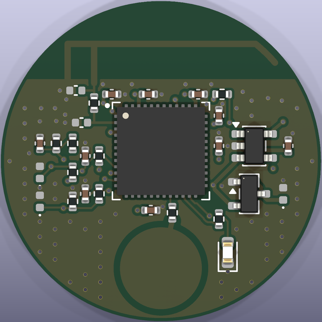 | 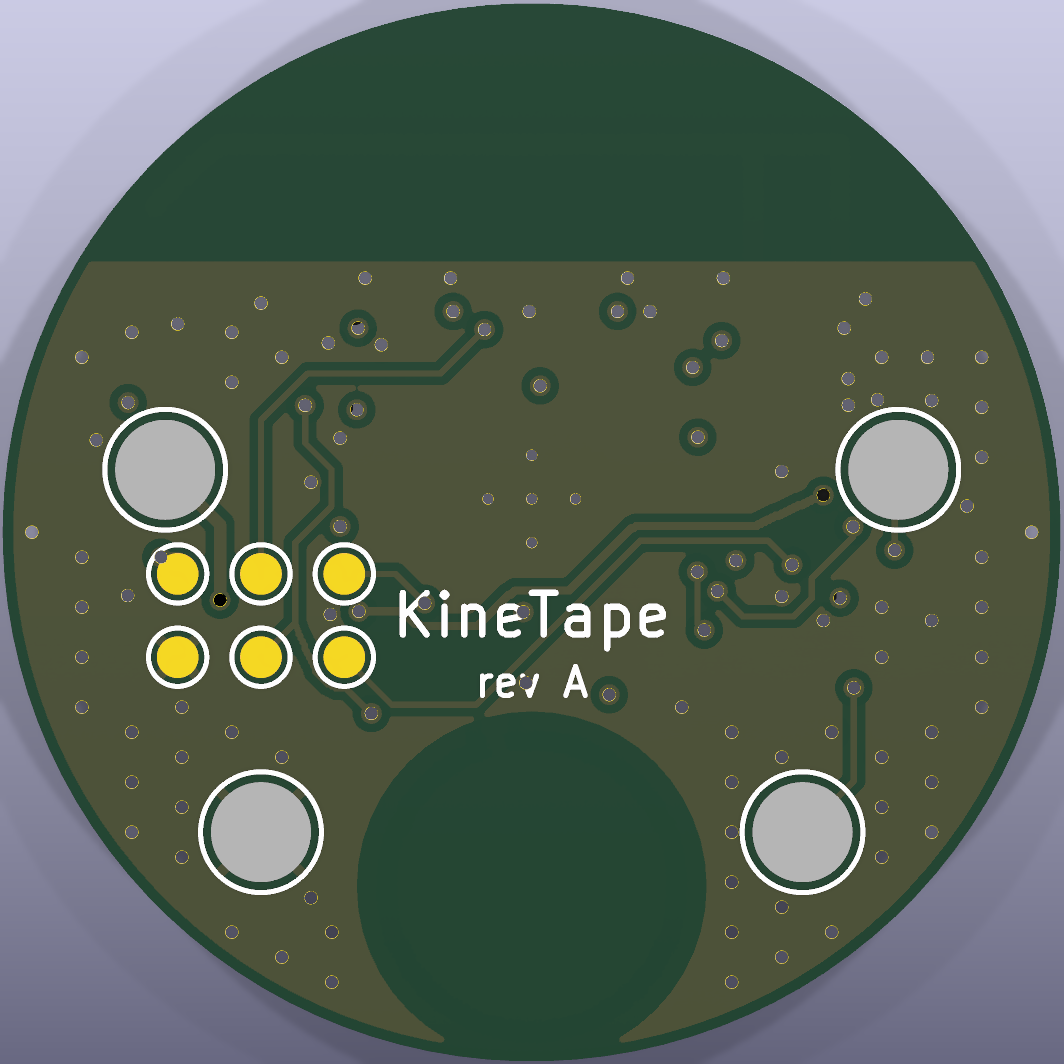 |
Status: schematic ERC-clean; board fully routed, 0 DRC violations / 0 unconnected / 0 schematic-parity errors (KiCad 10.0.7, all severities). Not yet fabricated or RF-tested — see Before you order.
| Block | Parts | Notes |
|---|---|---|
| MCU | U1 ESP32-PICO-V3-02 (LGA-48, 7×7 mm) | Classic ESP32 + 8 MB flash + 2 MB PSRAM + crystal in one package, so the existing esp32dev firmware runs. |
| Antenna | AE1 printed inverted-F, R10 + C11/C12 pi network | IFA runs along the top edge (above the ground cut). C11/C12 are DNP until tuned. |
| Power | Q1 AO3401A, U2 ME6211 3.3 V LDO, C1/C3 | Battery comes from the tape (J1). Q1 = reverse-polarity protection. ME6211: 500 mA, VIN up to 6 V. |
| Battery sense | R1/R2 1 MΩ divider + C4 → GPIO35 | VBAT/2, ~2 µA drain. |
| Sensor | J3/J4 + R7, R8, R9, C10 | Same divider as the firmware README: 3V3 → sensor → GPIO34 with 10 kΩ to GND (+1 kΩ/100 nF RC filter). |
| Touch | TS1 Ø6.5 mm electrode, R6 470 Ω | Electrode on the top layer under solder mask; no copper under it on inner/bottom layers. |
| LED | LED1 green 0603, R5 470 Ω → GPIO2 | Same pin as the firmware. |
| ESD | D1–D3 (0402) on every tape contact | The contacts touch the tape and skin. |
| Contact | Net | Position (from centre, top view) |
|---|---|---|
| J1 | VBAT in (3.0–5.5 V) | (+8.8, +1.5) mm |
| J2 | GND | (+6.5, −7.2) mm |
| J3 | SENS_A (3.3 V via 100 Ω) | (−8.8, +1.5) mm |
| J4 | SENS_B (→ ADC) | (−6.5, −7.2) mm |
The pattern is deliberately asymmetric, so the puck can only mate one way. The tape needs four flat conductive pads (snaps, conductive fabric or foil) at these positions. Spring free height is 3.5 mm, working height 2.9 mm.
| GPIO | Function | vs current firmware |
|---|---|---|
| 34 | Sensor ADC (ADC1_CH6) | unchanged |
| 2 | Status LED | unchanged |
| 35 | Battery sense, VBAT/2 (ADC1_CH7) | new; matches the "Future" note in firmware/README.md |
| 13 | Touch button (T4, touchRead(13)) | new |
| 1 / 3 | UART0 TX / RX (programming pads) | unchanged |
| 0 / EN | Boot / reset (programming pads) | — |
The 2×3 pad grid on the bottom (Ø1.0 mm, 2.0 mm pitch) is for a pogo-pin jig plus a 3.3 V USB-UART adapter:
TP3 TXD  (4.5,-1.0)   TP4 RXD (6.5,-1.0)   TP1 3V3 (8.5,-1.0)
TP5 EN   (4.5,-3.0)   TP6 IO0 (6.5,-3.0)   TP2 GND (8.5,-3.0)
There is no auto-reset circuit. To enter the bootloader, hold IO0 to GND and pulse EN to GND, then flash
with pio run -t upload. To power the board for flashing, feed VBAT through J1. Back-feeding TP1 (3V3)
works but pushes current into the LDO output.
These are the things I could not verify from here. Each one should be checked rather than assumed.
firmware/README.md) decides battery life
far more than this board does.Everything is generated from scripts/design.py (parts, nets, placement).
Don't hand-edit the .kicad_* files and then rerun the scripts, because the scripts overwrite them.
Run with KiCad's Python from hardware/:
"C:/Program Files/KiCad/10.0/bin/python.exe" scripts/build.py    # footprints, schematic, placed board, fanout
"C:/Program Files/KiCad/10.0/bin/python.exe" scripts/route.py    # Freerouting + finishing router + stitching
"C:/Program Files/KiCad/10.0/bin/python.exe" scripts/export.py   # DRC gate, then fab/ outputs
route.py needs tools/freerouting.jar (Freerouting 1.9.0, Java 17; git-ignored). It briefly opens a
Freerouting window. Whatever Freerouting leaves unrouted, the grid router in scripts/finish.py
completes. export.py refuses to write outputs unless DRC and schematic parity are clean.
| Script | Does |
|---|---|
design.py | The circuit: every part, its LCSC number, pin → net, PCB position |
footprints.py | Custom footprints: ESP32-PICO LGA-48, IFA antenna, touch pad, spring contact |
schematic.py | Writes the .kicad_sch (net labels on every pin); KiCad's own netlist export is then checked against design.py |
build.py | Board outline, placement, pours, keepouts, locked RF route, power fanout and escape vias |
fanout.py / finish.py | Clearance-checked via fanout; grid A* router for leftovers |
export.py | Gerbers + drill zip, JLCPCB BOM/CPL, schematic PDF, STEP |
fab/kinetape_puck_gerbers.zip. Set 4 layers, 1.0 mm, ENIG (recommended for the LGA and the
spring contacts), and the default impedance-free stackup.fab/kinetape_puck_bom.csv and fab/kinetape_puck_cpl.csv, then check the
placement preview (see item 5 above).fab/kinetape_puck.step to design the enclosure. It has the antenna at the top edge,
and the touch electrode should sit under a thin (≤ 1.5 mm) plastic lid.| Qty | Value | Footprint | References |
|---|---|---|---|
| 6 | 100nF | Capacitor_SMD:C_0402_1005Metric | C2, C4, C6, C7, C8, C10 |
| 3 | 10k | Resistor_SMD:R_0402_1005Metric | R3, R4, R8 |
| 3 | 10uF | Capacitor_SMD:C_0402_1005Metric | C1, C3, C5 |
| 3 | ESD 7V | Diode_SMD:D_0402_1005Metric | D1, D2, D3 |
| 2 | 1M | Resistor_SMD:R_0402_1005Metric | R1, R2 |
| 2 | 470R | Resistor_SMD:R_0402_1005Metric | R5, R6 |
| 2 | DNP | Capacitor_SMD:C_0402_1005Metric | C11, C12 |
| 1 | 0R | Resistor_SMD:R_0402_1005Metric | R10 |
| 1 | 100R | Resistor_SMD:R_0402_1005Metric | R7 |
| 1 | 1k | Resistor_SMD:R_0402_1005Metric | R9 |
| 1 | 1uF | Capacitor_SMD:C_0402_1005Metric | C9 |
| 1 | 3V3 | TestPoint:TestPoint_Pad_D1.0mm | TP1 |
| 1 | AO3401A | Package_TO_SOT_SMD:SOT-23 | Q1 |
| 1 | EN | TestPoint:TestPoint_Pad_D1.0mm | TP5 |
| 1 | ESP32-PICO-V3-02 | KineTape:ESP32-PICO-V3-02_LGA48_7x7mm | U1 |
| 1 | GND | KineTape:SpringContact_Harwin_P70-1000045R | J2 |
| 1 | GND | TestPoint:TestPoint_Pad_D1.0mm | TP2 |
| 1 | Green | LED_SMD:LED_0603_1608Metric | LED1 |
| 1 | IFA 2.4GHz | KineTape:Antenna_IFA_2G4_Puck | AE1 |
| 1 | IO0 | TestPoint:TestPoint_Pad_D1.0mm | TP6 |
| 1 | ME6211C33M5G-N | Package_TO_SOT_SMD:SOT-23-5 | U2 |
| 1 | RXD | TestPoint:TestPoint_Pad_D1.0mm | TP4 |
| 1 | SENS_A | KineTape:SpringContact_Harwin_P70-1000045R | J3 |
| 1 | SENS_B | KineTape:SpringContact_Harwin_P70-1000045R | J4 |
| 1 | TXD | TestPoint:TestPoint_Pad_D1.0mm | TP3 |
| 1 | Touch | KineTape:TouchPad_D6.5mm | TS1 |
| 1 | VBAT | KineTape:SpringContact_Harwin_P70-1000045R | J1 |
schmidtmt/openmotorbridge
The comprehensive technical specification is split into 18 logically organized chapters:


Neurallabware/Airscope_toolbox
A 1-gram wireless mesoscope for cortex-wide, single-cell-resolution imaging during unrestricted behaviour


nibble-arts/railway-can
A system to control analogue model railways combining the advantages of analogue and digital.


SonDinh23/EMGBand-HandBionic
Full-stack 6-ch dry-electrode sEMG wearable (ESP32/BLE, 1 kHz/ch, JSON presets) with DC removal + HPF/LPF + Kalman DSP and dual-path gesture control (Amplitude thresholds + 6-ch Radar-shape matching) + Flutter app…
41 parts, built around the ESP32-PICO-V3-02, ME6211C33M5G-N and AO3401A. The full list of its parts is on this page, with links to each part's symbol and footprint where PCBKit's library has them.
From the matthewfcarlin-cloud/SEP_MJF repository on GitHub, at the commit this page was made from: the board is kinn/hardware/kinetape_puck.kicad_pcb and its schematic kinn/hardware/kinetape_puck.kicad_sch. PCBKit opens the board in the browser, with nothing to install.
Its repository states no licence, so its author keeps all rights: ask matthewfcarlin-cloud before reusing the design.