Feather STM32WB55
A KiCad design for an STM32WB55CGU6 Bluetooth development board in the Adafruit Feather form factor, with USB-C, STEMMA QT, optional QSPI flash, and an optional SWD debug connector.
WARNING: Work In Progress
This is a work in progress, it may not work at all. :)
Do not order the included fabrication files as a manufacturing release. The source audit corrected a D10-to-ground short in the PCB source; the historical Gerbers and drill files still predate that fix. Layout, footprint, stackup, and electrical/RF review remain necessary before regenerating a complete fabrication set.
Overview
I have several Adafruit Feather boards, and Adafruit handily publish the Feather Specification here to make your own.
I recently discovered the STM32WB series of microcontrollers which include Bluetooth connectivity and decided to build my own development board around it. This repository is my first attempt at designing it and builds upon the great work of several sources (see Acknowledgements below).
The ultimate goal is to get this board working and running CircuitPython, once working I may do another revision with a focus on enabling more of the low power features of the STM32WB series.
Features
- STM32WB55CGU6 microcontroller
- Adafruit Feather compatible, with USB-C
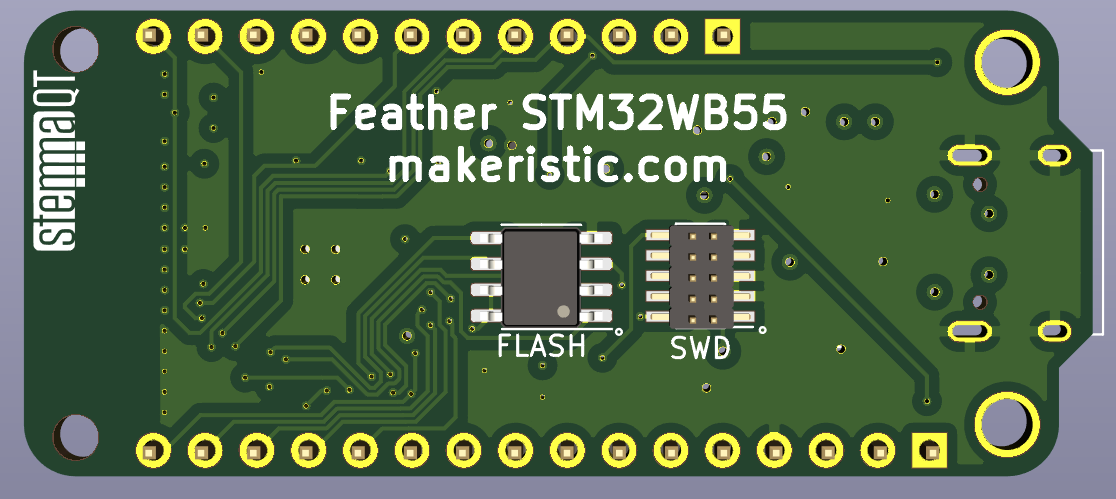
- (Optional) QSPI-Dual flash module can be soldered to the back
- (Optional) ARM SWD 10-pin debug connector can be soldered on the back
Notes
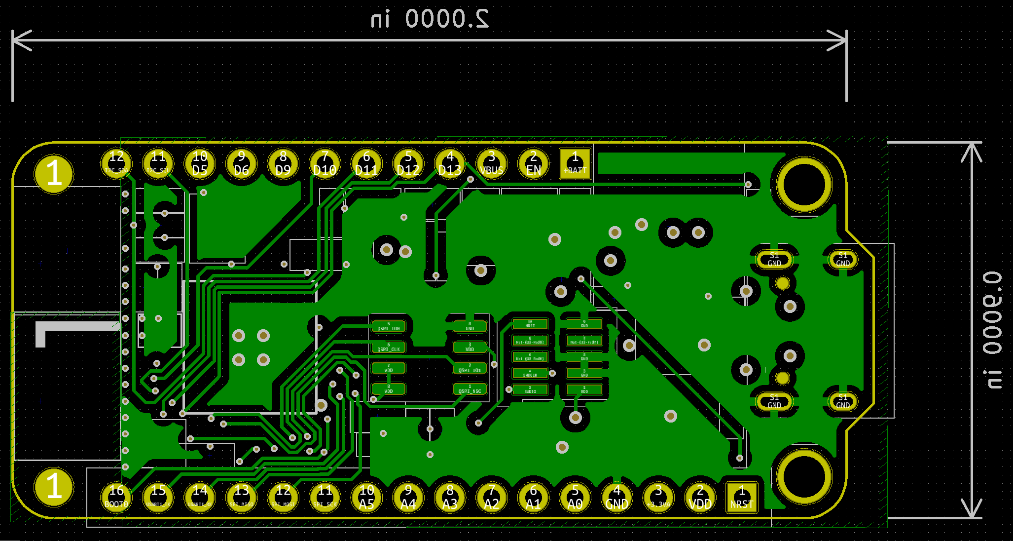
- The original fabrication notes specify a 4-layer board, 1mm thick with impedance-controlled traces, assuming the standard JLCPCB stackup. The committed PCB file currently records a thickness of 1.6mm; resolve this discrepancy with the board stackup before ordering.
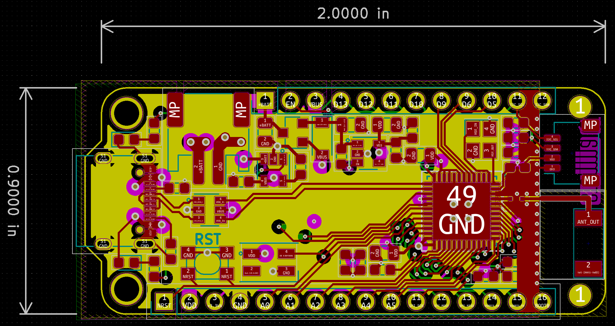
- I've tried to standardise on 0.2mm tracks for signals, 0.3mm tracks for power. VBUS and +BATT do have high-current tracks/pours to their respective pins to allow for powering things off-board like Neopixels.
- STMicroelectronics produce a custom matching network for this microcontroller MLPF-WB55-01E3, the recommended PCB layout has been implemented here.
- The Fractus Antenna has a recommended layout which is implemented here. The clearance area essentially takes up the entire tip of the board, though I have cheekily added the STEMMA QT connector, figuring it shouldn't have too big an impact.
- There is a lot of space around the center of the board, this is semi-intentional so I can extend the design with sensors, or an additional button.
- You can find my custom footprints etc. here Makeristic-KiCad-Library
Repository contents
Open or modify the design
- Clone the repository and open
Feather_STM32WB55.pro in KiCad. The PCB records KiCad 5.1.7; the .pro and .sch files are legacy formats. Import into a copy if using a newer KiCad release.
- Install the corresponding KiCad standard libraries and clone the Makeristic library alongside this repository. The project tables resolve that sibling checkout and the recovered board-local STM32/switch libraries. Keep the committed cache with the schematic so historical symbols remain available.
- Resolve library warnings before editing. ANT1 and FL1 now have qualified Makeristic footprint identifiers, and their 3D-model paths plus the STM32 model path resolve through the sibling checkout. The library notes describe the recovery and its limits; restored assets have not been independently redesigned or electrically verified.
- Review the RF layout, power path, stackup, and design-rule results before fabrication. Refill zones after source edits, then regenerate exports only after resolving the audit findings. Existing images and fabrication files remain historical snapshots.
Nightly KiCad netlist checks need the audit's cache-only export procedure: globally resolving the legacy USB symbol in nightly 10.99.0 omitted its shield pin from the export. No symbol/wiring workaround or bulk format migration was applied.
CircuitPython support remains the original project goal. No application firmware, flashing guide, or electrical/RF test report is included, and successful operation is not established by the files in this repository.
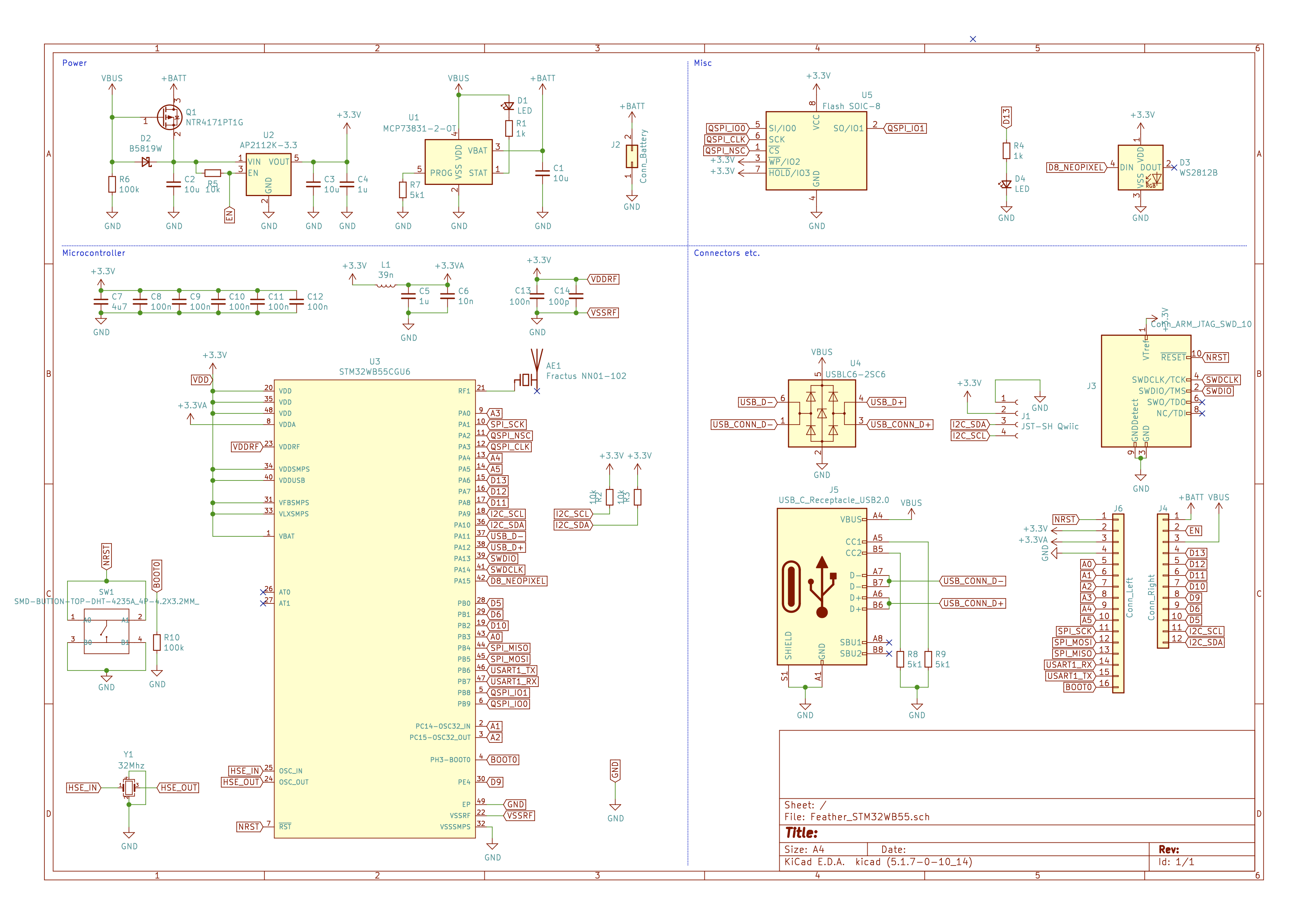
Schematic
PCB
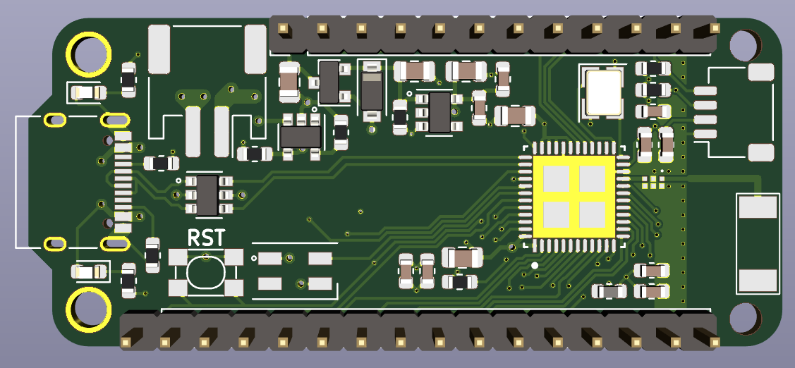
3D Render
TODO
- Improve the layout, potentially reassigning GPIO pins to simplify the traces
Acknowledgements
Feedback and related projects
Use Issues for questions, build reports, missing-library information, or design corrections. Include the commit, KiCad version, and relevant component references. For design pull requests, explain the circuit change and identify any regenerated fabrication files.
Related projects: Feather USB-C template, STUSB4500 breakout, and Makeristic-KiCad-Library.
Licence
Michael Cutler's original design work and documentation are available under the MIT licence. Vendor PDFs in datasheets/, third-party symbols, footprints and models (including embedded, recovered, and cached library elements), and third-party marks retain their respective owners' terms. KiCad symbols retain CC BY-SA 4.0 with the KiCad exception. The MIT grant does not relicense those materials or imply endorsement by the acknowledged organisations.


