

4 layers99 × 53.3 mm
PSLab
fossasia/pslab-hardware
PSLab Hardware Design and Schematics https://pslab.io
199 parts1.7kApache-2.0

A split wireless 36 key keyboard powered by the Seeed XIAO Nrf52840 with cherry ULP switches.
Ulp is an open-source printed circuit board by maker-lukas, from the maker-lukas/40-ish-ulp repository on GitHub, published under the CERN-OHL-S-2.0 licence. It is a 2-layer board of 103.1 × 82.2 mm with 53 parts on 42 nets, routed with 588 tracks and 86 vias.
It is built around the WS2812B. Its parts include 20 switches, 19 diodes, 2 connectors, 1 capacitor and 1 IC. It belongs with the nRF52 and nRF5x boards of this library.
A split wireless 36 key keyboard powered by the Seeed XIAO Nrf52840 with cherry ULP switches.


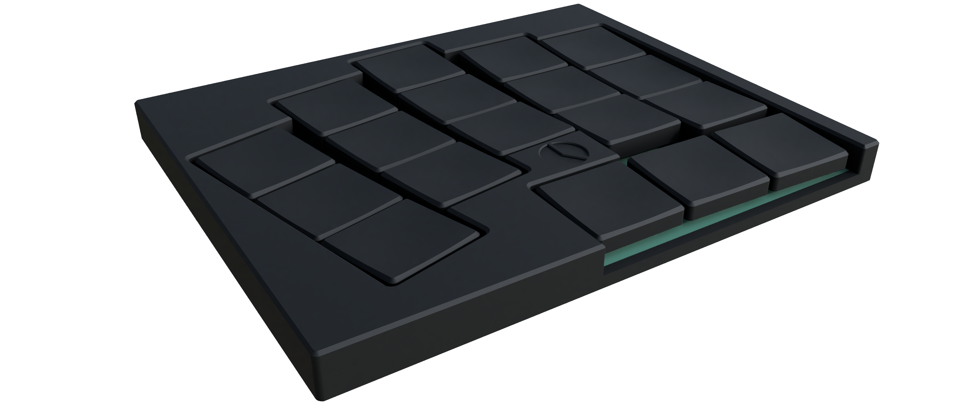
40%ish ulp is a split, ultra low profile keyboard with a 36 key layout, which is great when you are traveling or like a clean and slim build on your desk. It's only 8.25mm thick, with a huge battery so you won't have to charge it every day. It even has a status LED to tell you when the battery is low. Being wireless, it can connect to any device. Using ZMK firmware, you can customize your layout on the fly inside your browser, and its really power efficient!
| Part | Qty | Specification | Price | Link |
|---|---|---|---|---|
| MCU | 2 | Seeed XIAO nRF52840 | $26.18 | mauser.pt |
| Switches (pack of 10) | 4 | Cherry ULP | $41.63 | keeb.supply |
| PCBs | 5 | Reversible, MOQ 5 | $11.06 | jlcpcb.com |
| Batteries | 2 | 307095, 5000mAh battery | $16.23 | aliexpress.com |
| Diodes | 36 | SOD-123 | $1.57 | aliexpress.com |
| Power Switch | 2 | MK-12C02 | $0.87 | aliexpress.com |
| Reset Switch | 2 | EVQ-PUL02K | $1.87 | aliexpress.com |
| LEDs | 2 | WS2812B | $1.14 | aliexpress.com |
| Case | 2 | $6.42 | jlc3dp.com | |
| Keycaps | 36 | Resin Printed | $37.46 | jlc3dp.com |
| Magnets | 8 | 5x2mm round magnets | $2.88 | aliexpress.com |
| Total | $147.31 |
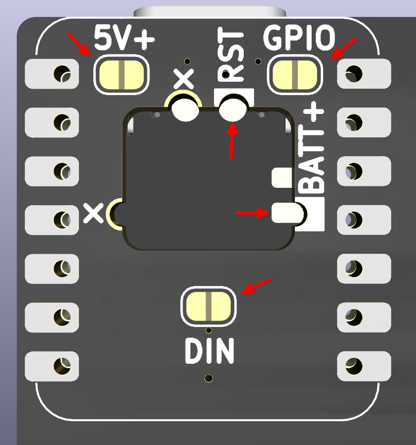
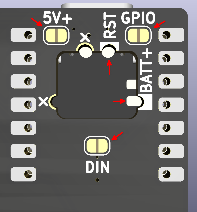
Because the PCB is reversible, some of the pins need to be reversed by bridging solder jumpers. Solder all 5 points shown in the images below for each side.
| Left | Right |
|---|---|
 |  |
Blueprint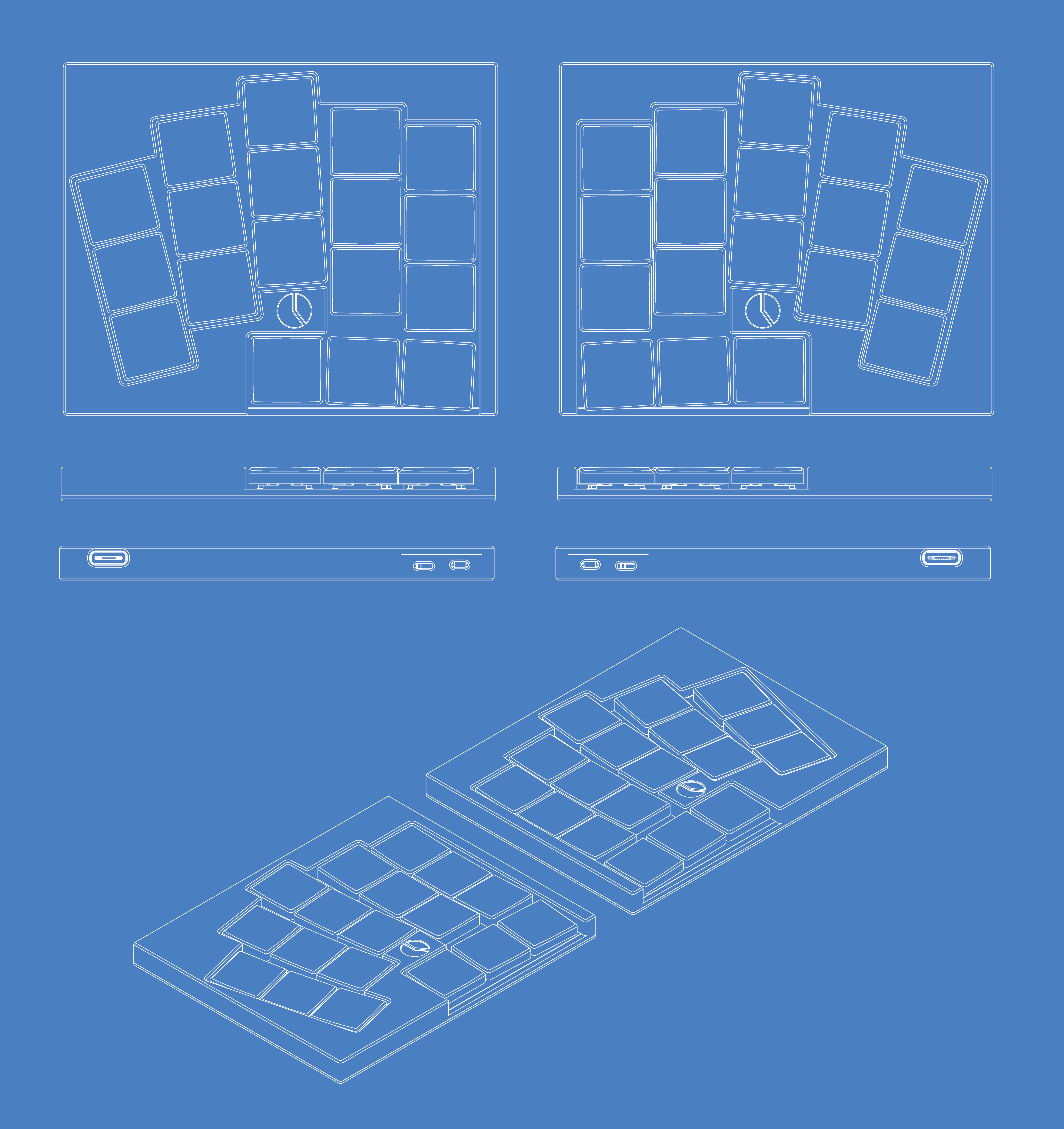 |
Schematic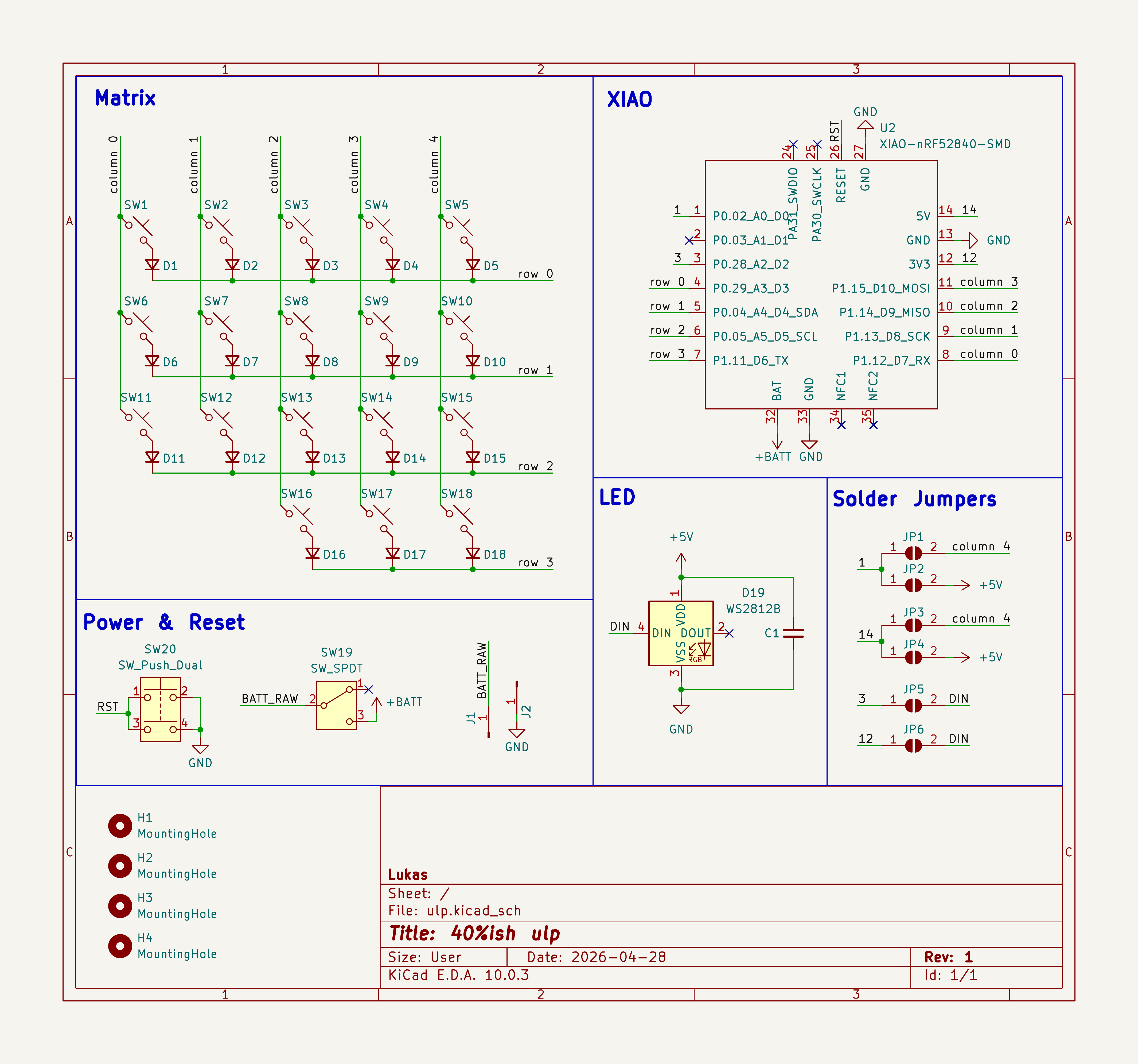 |
PCB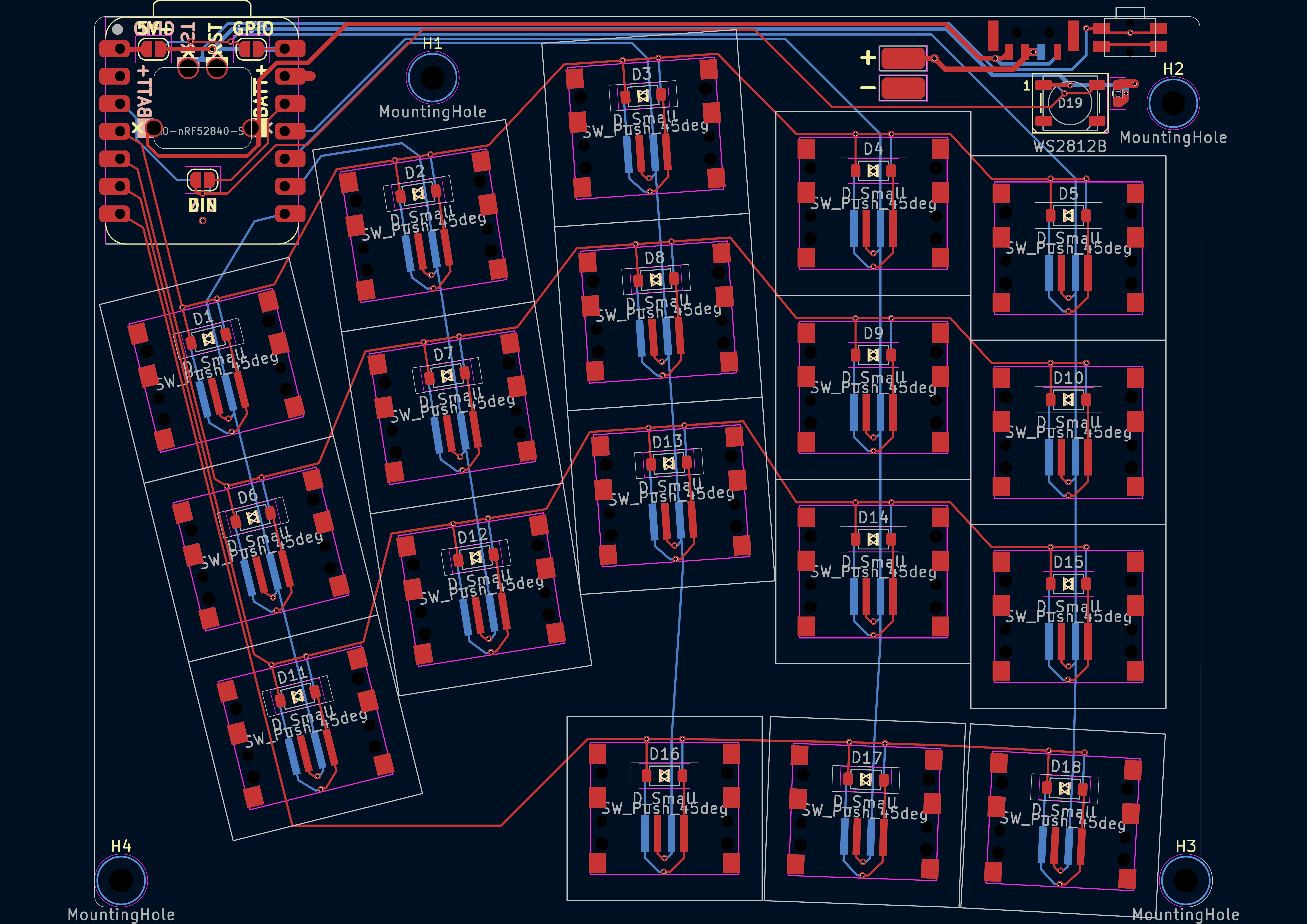 |
Zine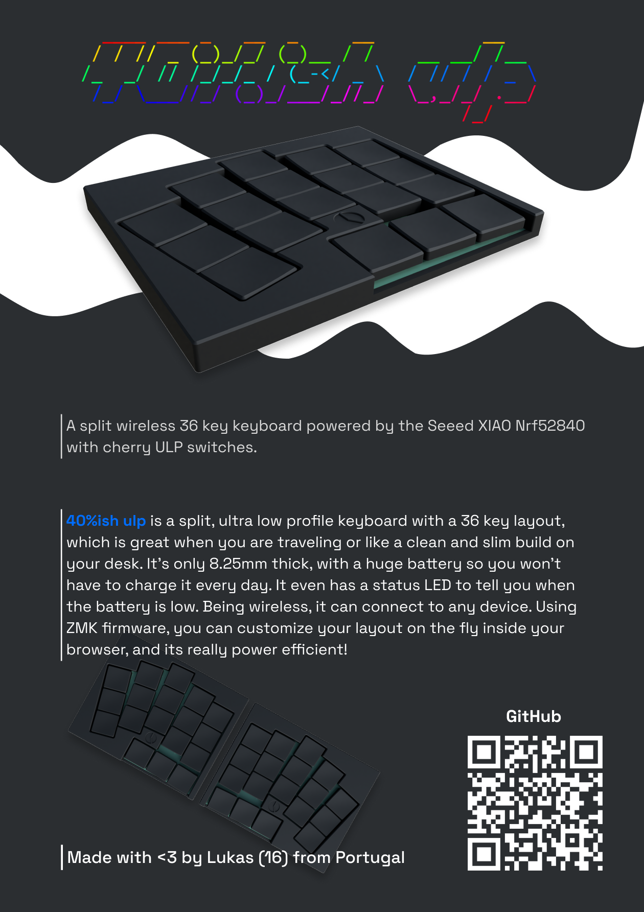 Full PDF |
| Qty | Value | Footprint | References |
|---|---|---|---|
| 18 | D_Small | reversible:D_SOD-123_Reversible | D1, D2, D3, D4, D5, D6, D7, D10, D11, D12, D13, D14, D15, D16, D17, D18 +2 |
| 18 | SW_Push_45deg | Cherry_ULP:Cherry_ULP_SMD_Double_Sided | SW1, SW2, SW3, SW4, SW5, SW6, SW7, SW10, SW11, SW12, SW13, SW14, SW15, SW16, SW17, SW18 +2 |
| 6 | SolderJumper_2_Open | Jumper:SolderJumper-2_P1.3mm_Open_RoundedPad1.0x1.5mm | JP1, JP2, JP3, JP4, JP5, JP6 |
| 4 | MountingHole | MountingHole:MountingHole_2.2mm_M2 | H1, H2, H3, H4 |
| 2 | Conn_01x01_Pin | reversible:TestPoint_Pad_2.0x4.0mm_Reversible | J1, J2 |
| 1 | C_Small | reversible:C_0603_1608Metric_Reversible | C1 |
| 1 | SW_Push_Dual | reversible:SW_Push_SPST_EVQ-PU_Reversible | SW20 |
| 1 | SW_SPDT | reversible:SW_SPDT_MSK-12C02_Reversible | SW19 |
| 1 | WS2812B | reversible:LED_WS2812B_PLCC4_5.0x5.0mm_P3.2mm_Reversible | D19 |
| 1 | XIAO-nRF52840-SMD | reversible:MODULE_Seeed_XIAO_nRF52840_THT_Reversible | U2 |
fossasia/pslab-hardware
PSLab Hardware Design and Schematics https://pslab.io

FrameworkComputer/ExpansionCards
Reference designs and documentation to create Expansion Cards for the Framework Laptop


PrintersForAnts/Micron
If you want to purchase full kits there are 3 available (Kits are slowly updating to R1 hardware just make sure to double check the included hardware in your kit and if you have any questions reach out in the discord)


It measures 103.1 × 82.2 mm and has 2 copper layers, 1.6 mm thick.
53 parts, built around the WS2812B. The full list of its parts is on this page, with links to each part's symbol and footprint where PCBKit's library has them.
From the maker-lukas/40-ish-ulp repository on GitHub, at the commit this page was made from: the board is pcb/ulp.kicad_pcb and its schematic pcb/ulp.kicad_sch. PCBKit opens the board in the browser, with nothing to install.
Its repository publishes it under the CERN-OHL-S-2.0 licence: you may reuse it on that licence's terms (keep the author's notice, and for a copyleft licence share your changes alike).