2 layers69.1 × 77.1 mm

 lzyang2000/PCB-Projects1
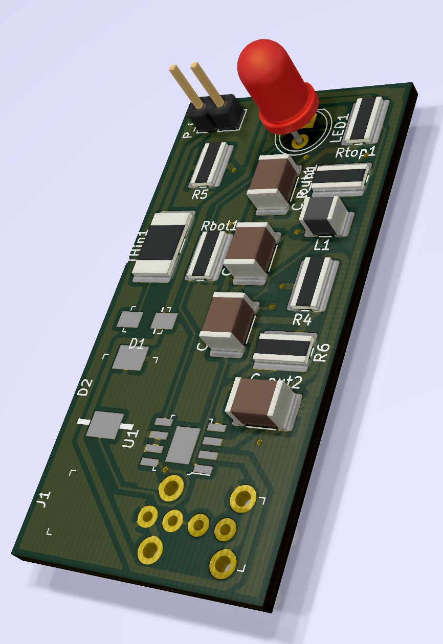
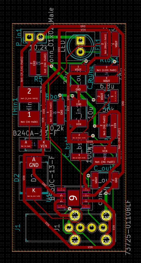
Wireless proj is an open-source printed circuit board by lzyang2000, from the lzyang2000/PCB-Projects repository on GitHub. It is a 2-layer board of 77.9 × 54.6 mm with 21 parts on 12 nets, routed with 94 tracks and 10 vias.
Its parts include 5 resistors, 5 connectors, 3 diodes, 2 capacitors and 2 ICs.
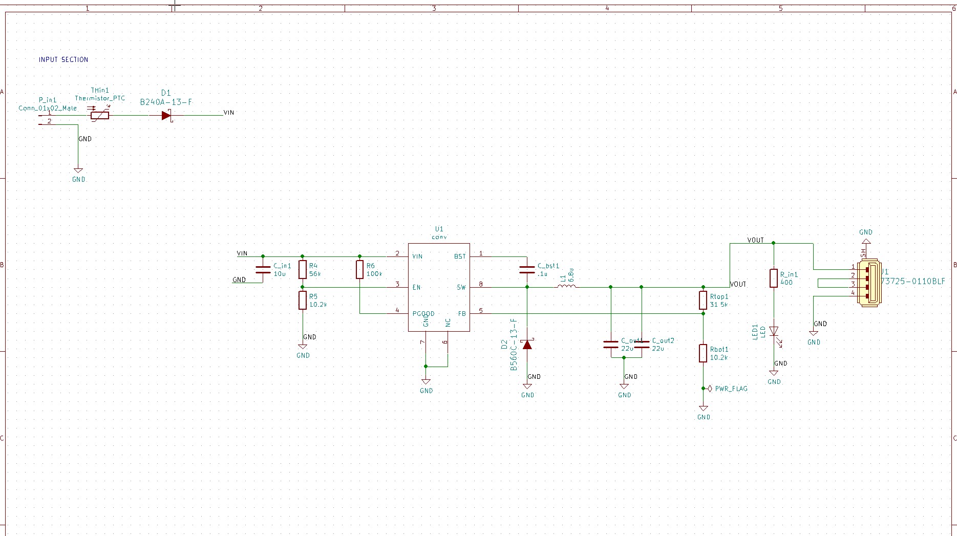
Takes input of 9-18V DC and outputs power compliant with USB Battery Charging 1.2.
BOM
| Qty | Value | Footprint | References |
|---|---|---|---|
| 3 | 200 | Resistor_SMD:R_2010_5025Metric_Pad1.52x2.65mm_HandSolder | R2, R3, Rl1 |
| 2 | 10u | Capacitor_SMD:C_1812_4532Metric_Pad1.30x3.40mm_HandSolder | C1, C2 |
| 2 | Conn_01x01_Male | Connector_PinHeader_2.54mm:PinHeader_1x01_P2.54mm_Horizontal | J2, J3 |
| 2 | Conn_01x02_Male | Connector_PinHeader_2.54mm:PinHeader_1x02_P2.54mm_Horizontal | J1, P_in1 |
| 1 | 1 | Resistor_SMD:R_2010_5025Metric_Pad1.52x2.65mm_HandSolder | R1 |
| 1 | 4.99k | Resistor_SMD:R_2010_5025Metric_Pad1.52x2.65mm_HandSolder | R4 |
| 1 | Conn_01x02_Female | Connector_PinHeader_2.54mm:PinHeader_1x02_P2.54mm_Vertical | J4 |
| 1 | D_Schottky | Diode_SMD:D_3220_8050Metric_Pad2.65x5.15mm_HandSolder | D2 |
| 1 | D_Schottky_ALT | Diode_SMD:D_2512_6332Metric_Pad1.52x3.35mm_HandSolder | D1 |
| 1 | LED | LED_THT:LED_D5.0mm | LED1 |
| 1 | LM7805CT_Obsolete | Connector:FanPinHeader_1x03_P2.54mm_Vertical | U2 |
| 1 | LOGO | logos:bac-logo | G*** |
| 1 | LOGO | logos:ieee-logo-inv | G*** |
| 1 | LT6106 | Package_TO_SOT_SMD:SOT-23-8 | U1 |
| 1 | Q_NMOS_DGS | Package_TO_SOT_THT:TO-3P-3_Horizontal_TabDown | M1 |
| 1 | Thermistor | Resistor_SMD:R_2010_5025Metric_Pad1.52x2.65mm_HandSolder | TH1 |
It measures 77.9 × 54.6 mm and has 2 copper layers, 1.6 mm thick.
21 parts. The full list of its parts is on this page, with links to each part's symbol and footprint where PCBKit's library has them.
From the lzyang2000/PCB-Projects repository on GitHub, at the commit this page was made from: the board is wireless_proj/wireless_proj.kicad_pcb. PCBKit opens the board in the browser, with nothing to install.
Its repository states no licence, so its author keeps all rights: ask lzyang2000 before reusing the design.


gusmanb/logicanalyzer
24 channel, 100Msps logic analyzer hardware and software

mntmn/amiga2000-gfxcard
MNT VA2000, an Open Source Amiga 2/3/4000 Graphics Card (Zorro II/III), written in Verilog


hackclub/OnBoard
💡 Join 1,000 teenagers and make your first PCB with a $100 grant!

drandyhaas/KiCadRoutingTools
A set of Python/Rust tools to aid routing in KiCad

Arrow-air/project-quiver
Project Quiver documentation, designs, and project artifacts.

