Skip to the content
PCBKitNew board
4 layers48.5 × 16.3 mmCoupler test, the printed circuit board in 3D

Coupler test

loxodes/vna205

Under development open hardware microwave vector network analyzer

Size
48.5 × 16.3 mm
Copper layers
4
Thickness
1.6 mm
Parts
4
Nets
5
Pads
162
Tracks, vias
10, 0
Pours
2
Routed
Yes
KiCad
KiCad 4
Created
22 Apr 2016
Updated
31 Dec 2023

Overview

Coupler test is an open-source printed circuit board by loxodes, from the loxodes/vna repository on GitHub. It is a 4-layer board of 48.5 × 16.3 mm with 4 parts on 5 nets, routed with 10 tracks and 0 vias.

It belongs with the radio and wireless and sensors and measurement boards of this library.

README

README.md

Open Hardware Vector Network Analyzer

I'm developing a proof of concept two port microwave vector network analyzer. The project is under developent. Ongoing documentation and logs are located on a hackaday.io project page.

Usage

This project is still under development, y'all probably don't want to try reproducing it yet. Two port measurements to 14 GHz work, a redesign for operation out to 36 GHz is in progress.

Hardware Design

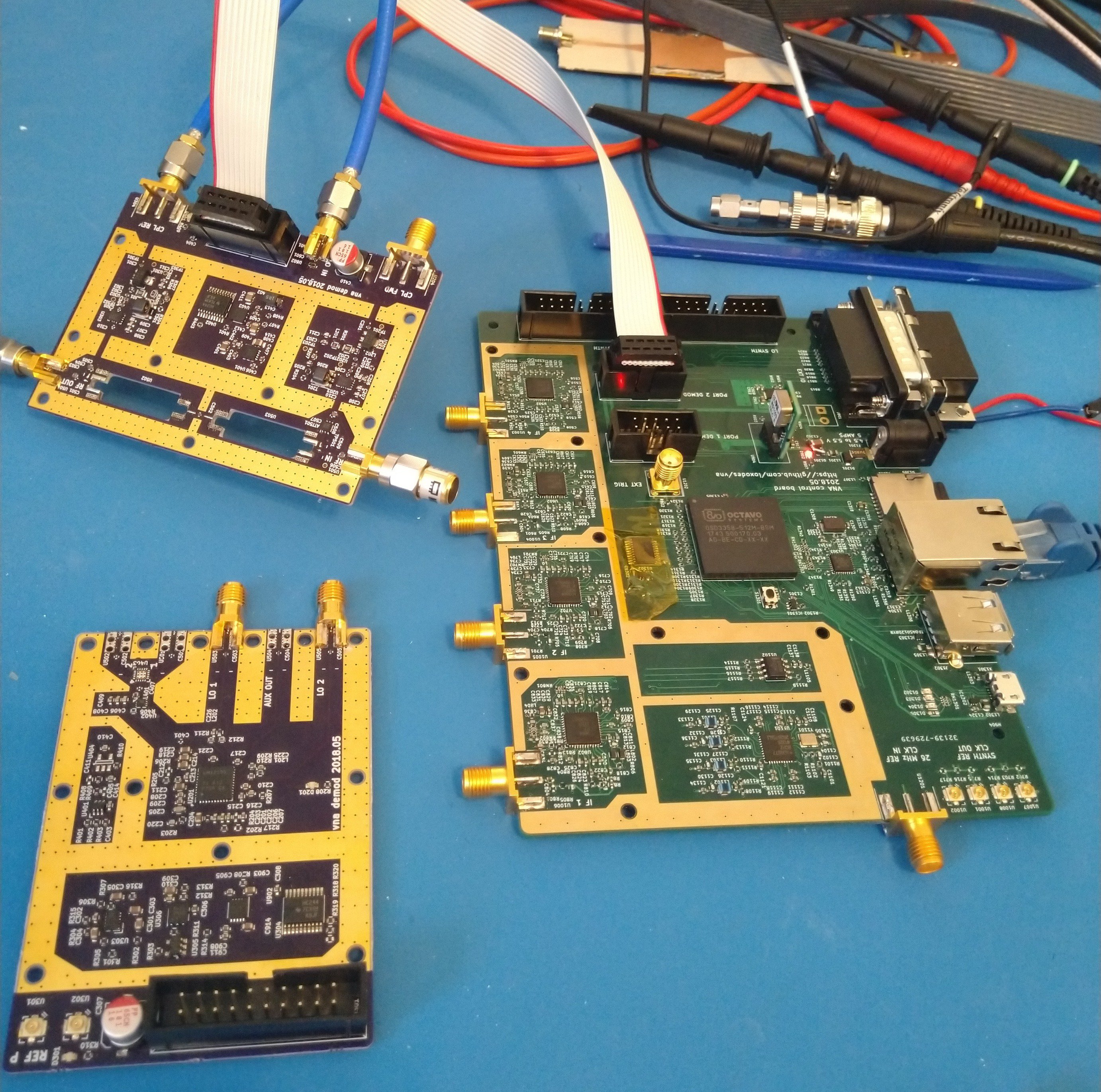
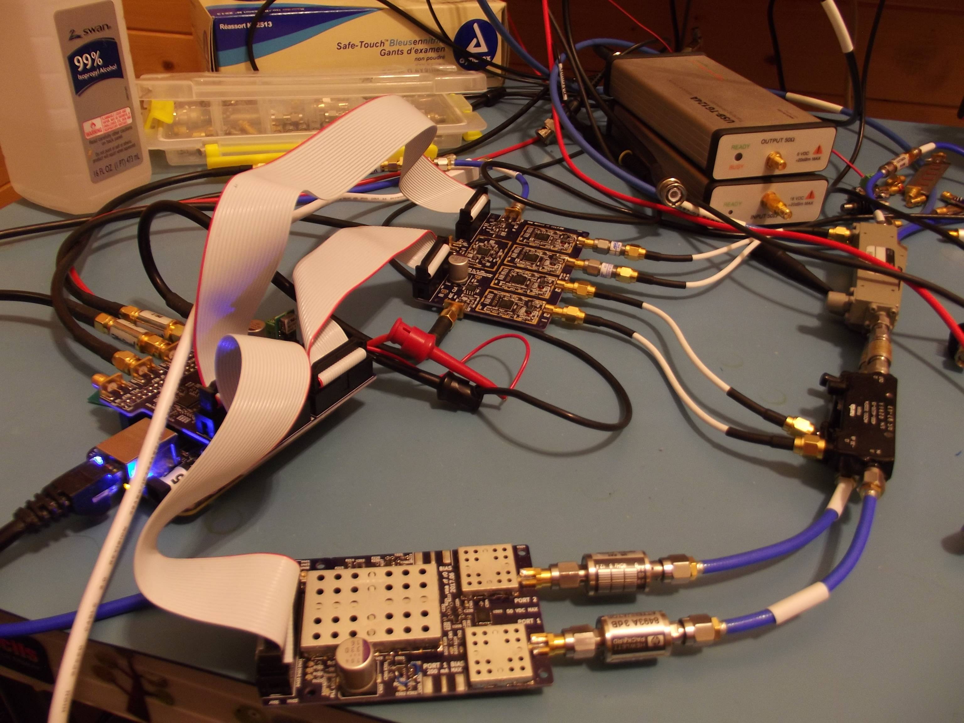
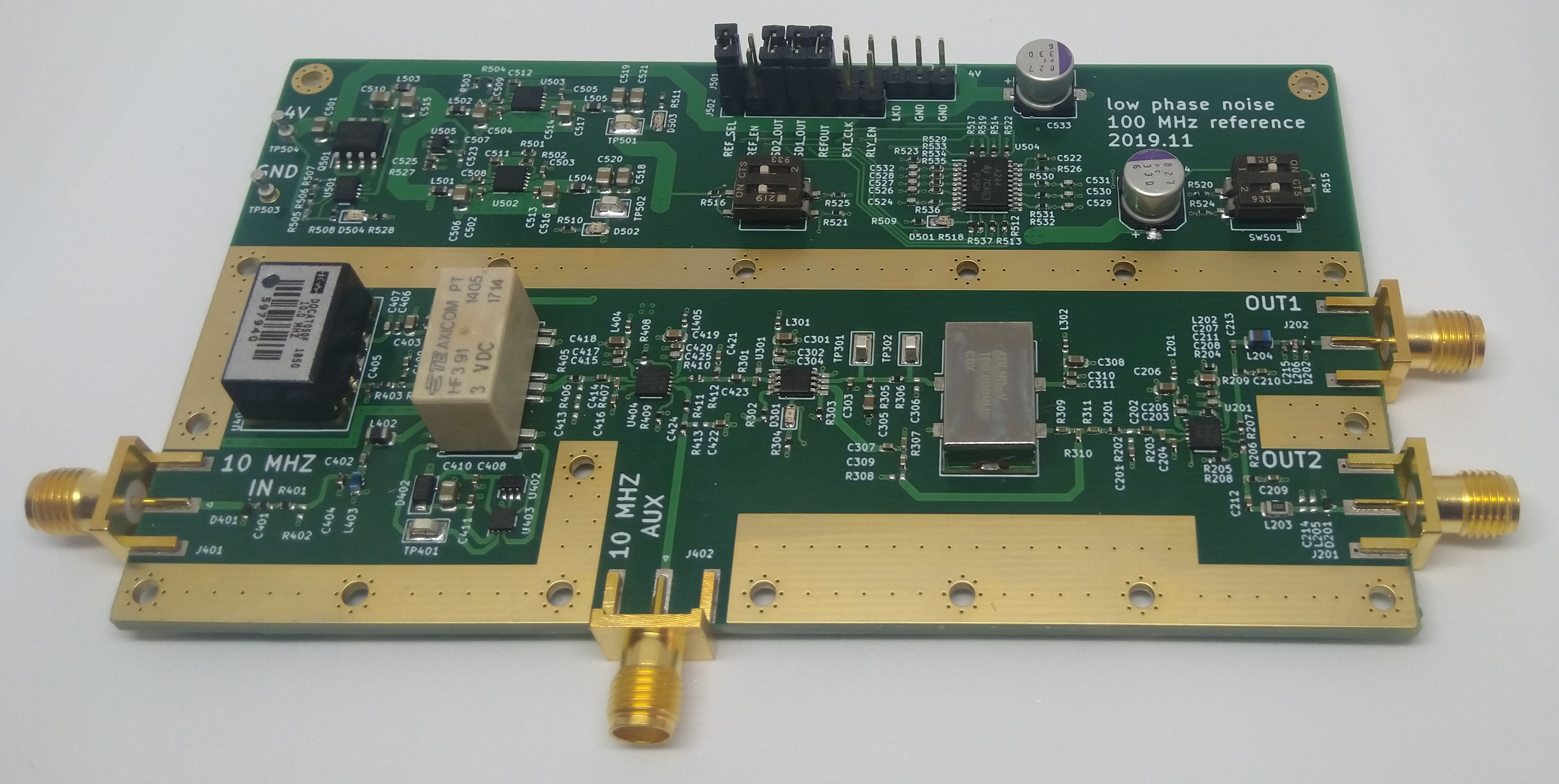
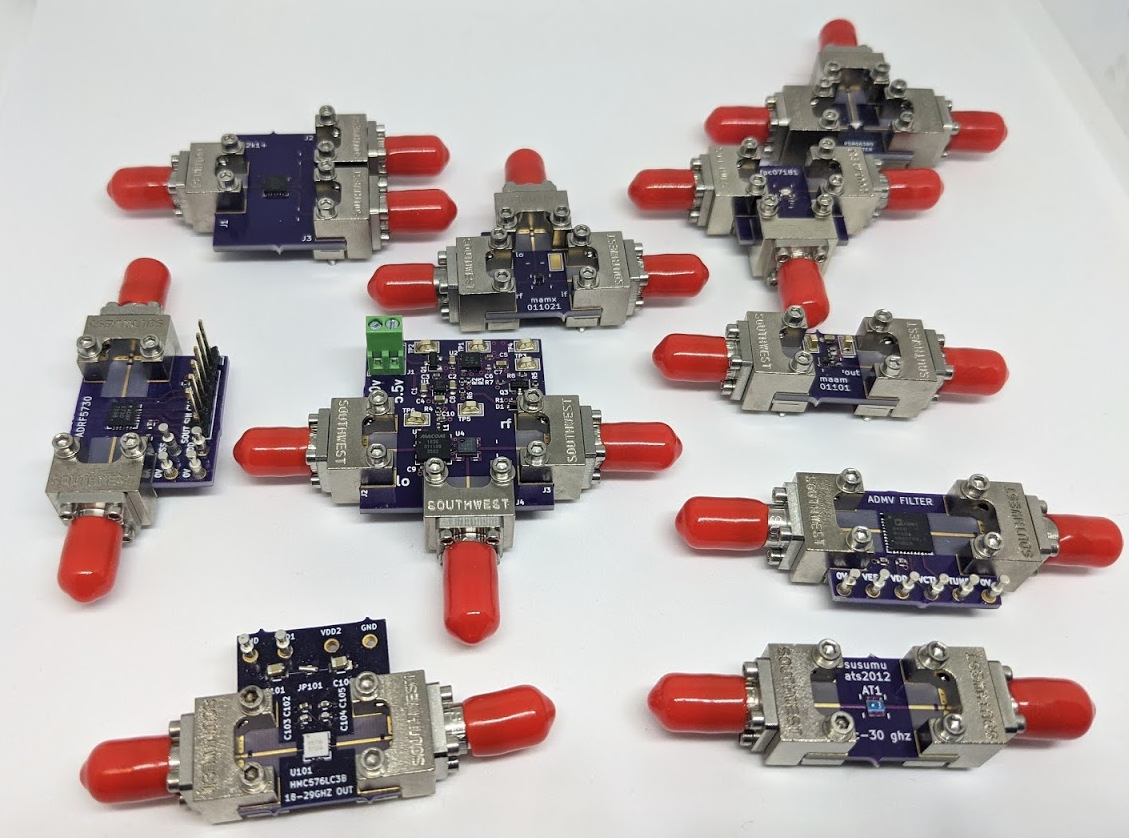
See breakouts and hardware for various modules developed for the network analyzer. picture of VNA R1 picture of VNA picture of VNA reference picture of mm modules

Software Design

See the software directory for scraps of software written for testing VNA modules.

License

Unless otherwise noted, all work is under a MIT license.

Contact

Feel free to contact me at arcticmicrowave@gmail.com or loxodes on irc.freenode.net

Parts

4
QtyValueFootprintReferences
3CONN_SMA_2GNDvna_footprints:SMA_901-10512_6p7MIL_FR408_CPW_LAUNCHU101, U103, U104
1resistive_bridgevna_footprints:resistive_bridge_osh_fr408_ustripU102

Questions

How big is the Coupler test PCB?

It measures 48.5 × 16.3 mm and has 4 copper layers, 1.6 mm thick.

What parts does the Coupler test use?

4 parts. The full list of its parts is on this page, with links to each part's symbol and footprint where PCBKit's library has them.

Where can I download the Coupler test KiCad files?

From the loxodes/vna repository on GitHub, at the commit this page was made from: the board is breakouts/coupler_test/coupler_test.kicad_pcb. PCBKit opens the board in the browser, with nothing to install.

Can I use the Coupler test design in my own project?

Its repository states no licence, so its author keeps all rights: ask loxodes before reusing the design.

More from loxodes/vna

12
  • 4 layers66.5 × 93.5 mmVna demod, the printed circuit board in 3D

    Vna demod

    loxodes/vna

    Under development open hardware microwave vector network analyzer

    721 parts205
  • 4 layers78.5 × 55.5 mmVna r1 demod, the printed circuit board in 3D

    Vna r1 demod

    loxodes/vna

    Under development open hardware microwave vector network analyzer

    588 parts205
  • 4 layers105 × 140 mmVna r1, the printed circuit board in 3D

    Vna r1

    loxodes/vna

    Under development open hardware microwave vector network analyzer

    555 parts205
  • 4 layers78 × 49 mmVna rf, the printed circuit board in 3D

    Vna rf

    loxodes/vna

    Under development open hardware microwave vector network analyzer

    527 parts205
  • 4 layers78 × 56 mmVna r1 synth, the printed circuit board in 3D

    Vna r1 synth

    loxodes/vna

    Under development open hardware microwave vector network analyzer

    485 parts205
  • 6 layersVna mm synth, the printed circuit board in 3D

    Vna mm synth

    loxodes/vna

    Under development open hardware microwave vector network analyzer

    435 parts205
  • 4 layers43.2 × 35.6 mmDoubler switch, the printed circuit board in 3D

    Doubler switch

    loxodes/vna

    Under development open hardware microwave vector network analyzer

    363 parts205
  • 4 layers97.1 × 32.8 mmFrequency synth, the printed circuit board in 3D

    Frequency synth

    loxodes/vna

    Under development open hardware microwave vector network analyzer

    278 parts205
  • 4 layers29 × 36 mmAdrf5020 breakout, the printed circuit board in 3D

    Adrf5020 breakout

    loxodes/vna

    Under development open hardware microwave vector network analyzer

    258 parts205
  • 4 layers31.2 × 44 mmSot89 amp test, the printed circuit board in 3D

    Sot89 amp test

    loxodes/vna

    Under development open hardware microwave vector network analyzer

    251 parts205
  • 4 layers115.5 × 66 mmVna mm ref, the printed circuit board in 3D

    Vna mm ref

    loxodes/vna

    Under development open hardware microwave vector network analyzer

    229 parts205
  • 4 layers31.3 × 23.5 mmPe42520 breakout, the printed circuit board in 3D

    Pe42520 breakout

    loxodes/vna

    Under development open hardware microwave vector network analyzer

    217 parts205

Similar boards

  • 4 layers33.7 × 12.4 mmDisplay eval short, the printed circuit board in 3D

    Display eval short

    byrantech/laptop

    anyon_e, a highly integrated, high end, open source laptop. Attempt the impossible.

    4 parts4.3kMIT
  • 4 layers78 × 40 mmAdd on template, the printed circuit board in 3D

    Add on template

    dotstartech/wall-panel

    Wall mounted 4 inch touch display panel with CM4 inside

    4 parts445
  • 4 layers27.5 × 25 mmVna amplifier, the printed circuit board in 3D

    Vna amplifier

    azonenberg/starshipraider

    Open hardware test equipment

    4 parts193BSD-3-Clause
  • 4 layers80 × 40 mmInit file, the printed circuit board in 3D

    Init file

    Hongcheng-Gao/EngiWorld

    Engiworld: What Can Frontier Agents Deliver in Professional Engineering Environments?

    4 parts52MIT
  • 4 layers44.5 × 59.5 mmBreadboard adapter, the printed circuit board in 3D

    Breadboard adapter

    OpenDevicePartnership/pico-de-gallo

    A tool for testing Embedded Rust drivers for discrete I2C/SPI components.

    4 parts21MIT
  • 4 layers28 × 17 mmJtag swd bridge, the printed circuit board in 3D

    Jtag swd bridge

    azonenberg/misc-devboards

    Miscellaneous prototype hardware that wasn't major enough to warrant a dedicated repo

    4 parts17BSD-3-Clause
  • 4 layers22 × 30 mmM.2 usd, the printed circuit board in 3D

    M.2 usd

    martonmiklos/m.2_microsd

    M.2 E key to micro SD adapter CAD files

    4 parts17
  • 4 layers15.2 × 43.8 mmProm, the printed circuit board in 3D

    Prom

    ronnyroy111/inboard386

    Reverse engineered schematics, PCB and logic equations for the Intel 386/PC accelerator

    4 parts16MIT