
2 layers63.3 × 15 mm
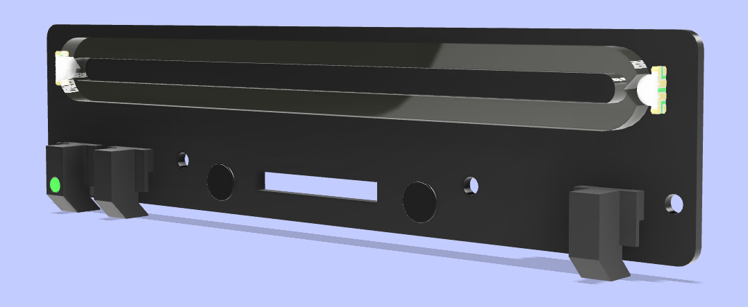
Ss front panel
loopj/short-stack
World's Smallest Nintendo Wii, using a trimmed motherboard and custom stacked PCBs
13 parts804
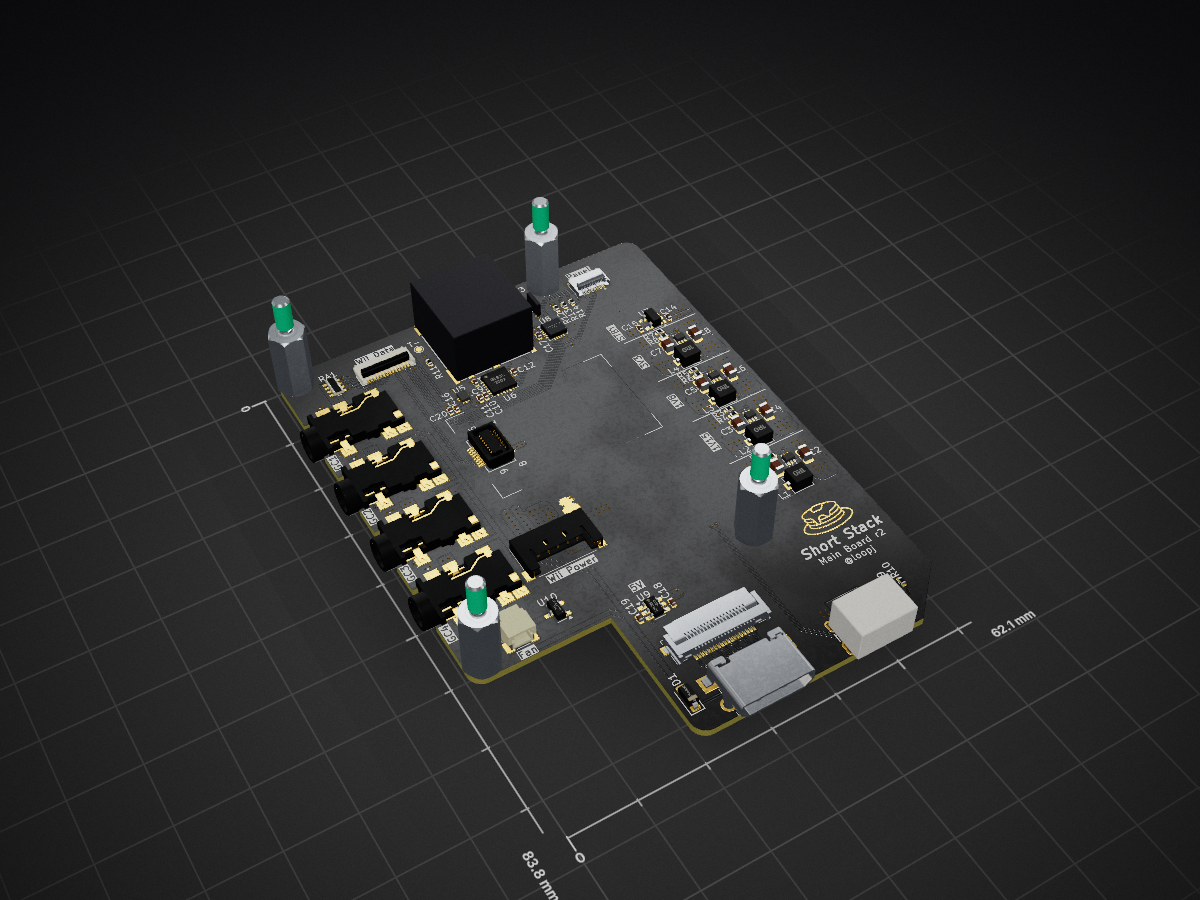
 loopj/short-stack804
World's Smallest Nintendo Wii, using a trimmed motherboard and custom stacked PCBs
Ss main board is an open-source printed circuit board by loopj, from the loopj/short-stack repository on GitHub. It is a 4-layer board of 62.1 × 83.8 mm with 69 parts on 105 nets, routed with 489 tracks and 318 vias.
It is built around the ATTINY1616-MN, TLV62585DRL and DRDC3105F-7, with the MIC5504-3.3YM5-TR, SIP32510DT and TMUXHS221NKGR among its other parts. Its parts include 20 capacitors, 14 resistors, 14 connectors, 10 ICs and 4 inductors. It belongs with the computers and single-board computers and retro computing and games boards and the AVR (ATmega, ATtiny) boards of this library.




Features · Size & Scale · Components · Build Guide · Special Thanks
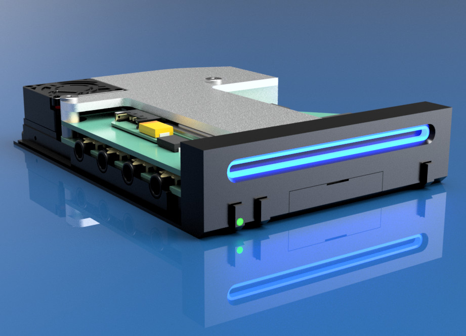
This is a 1:2.38 scale model of an original Nintendo Wii console, but since that is hard to visualize here are some other stats:
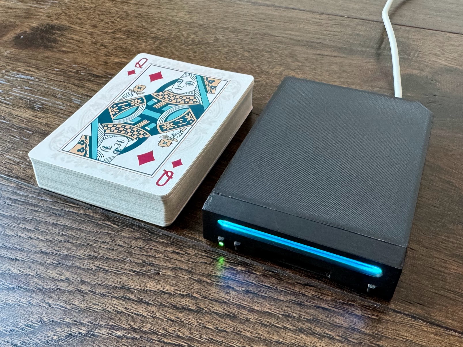
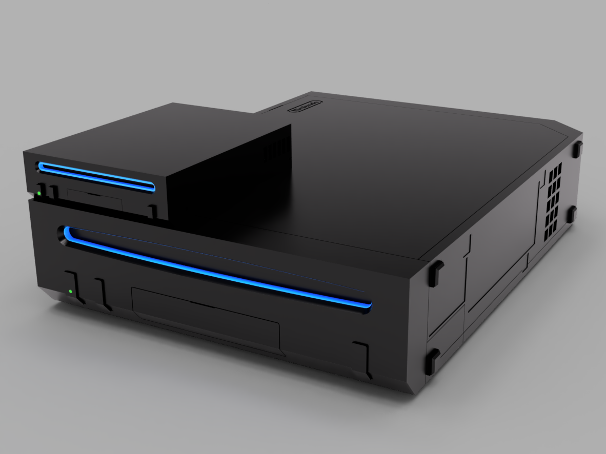
I'm pretty sure this sets the record for the smallest functional scale-model Wii console, but let me know if I'm wrong!
Yes! It is definitely possible to go smaller than this. My version of the Omega trim keeps all four main mounting holes, which makes it around 7mm wider than a classic Omega trim. Additionally Wesk has managed to get a Wii motherboard down to 52x52mm on his final destination trim, which is a a full 10mm narrower than my trim. I estimate you could reduce the volume by a further 25-30% without losing any functionality, but it would be an incredibly tight fit and tricky to assemble.
As the name implies, Short Stack is built from a stack of custom PCBs, and a custom heatsink, that are all designed to fit together in a compact and modular way.
Making a tiny build like this is made possible by trimming the Wii motherboard down to the bare essentials. The result is a board which is just 62x62mm, but still contains the CPU, GPU, RAM and flash memory.
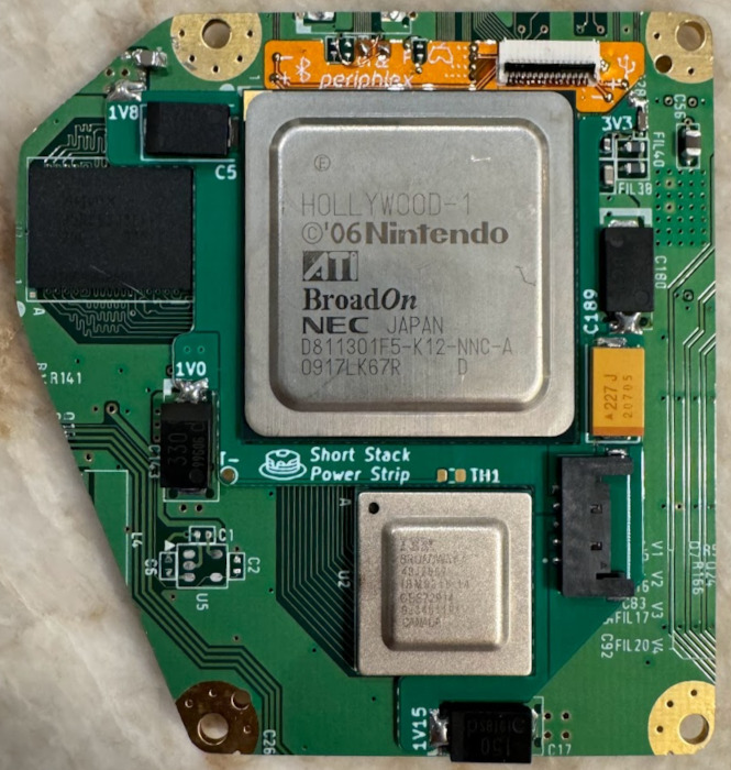
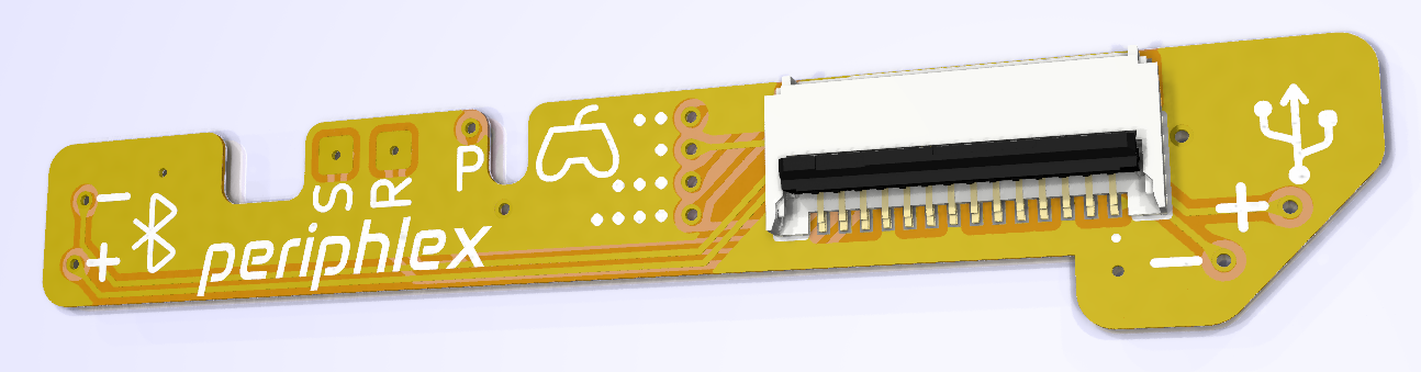
Since we removed the original power circuitry and trimmed off the USB, Bluetooth, and GameCube connectors, we need to provide power and data to the board another way. I designed a couple of boards which solder directly to the front of a trimmed Wii motherboard to provide power and data, which help avoid a tangled mess of wires.
The Wii Power Strip supplies power to the Wii motherboards using a Molex Pico-Lock connector, and additionally has footprints to help relocate of a couple of capacitors which are typically removed when trimming a Wii.
Periphlex is a flex PCB which breaks out the Bluetooth, USB and GameCube controller data lines, as well as the power, shutdown, and reset GPIOs. These are then made available via a 14-pin FFC connector. This approach replaces 11 magnet wires with a single, removable ribbon cable.
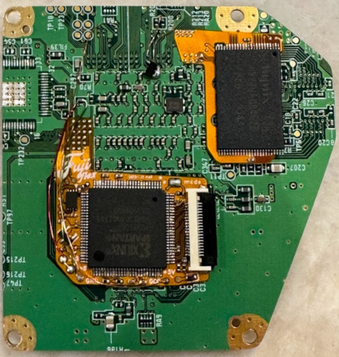
On the back of the motherboard, I'm using two open-source boards designed by the very talented YveltalGriffin. fujiflex provides digital A/V output using GCVideo, and nandFlex relocates the Wii's NAND memory chip, to enable the tight trim.
In addition to the modular boards on the motherboard, I designed two PCBs specific to Short Stack which provide the rest of the functionality for the console.
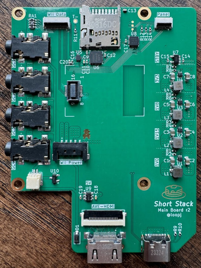
The main board PCB hosts the power regulators, USB to microSD logic, HDMI connector, GameCube ports, and a microcontroller for power management. A 14-pin ribbon cable connects this board to the Wii motherboard via Periphlex, and a power cable delivers power to the Power Strip.
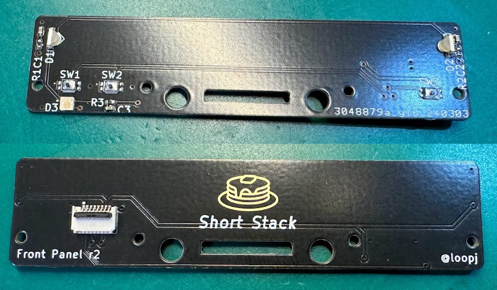
The front panel PCB hosts the power, reset, and sync buttons, as well as the power LED and disc slot LEDs. This board connects to the main board via a short 8-pin ribbon cable.
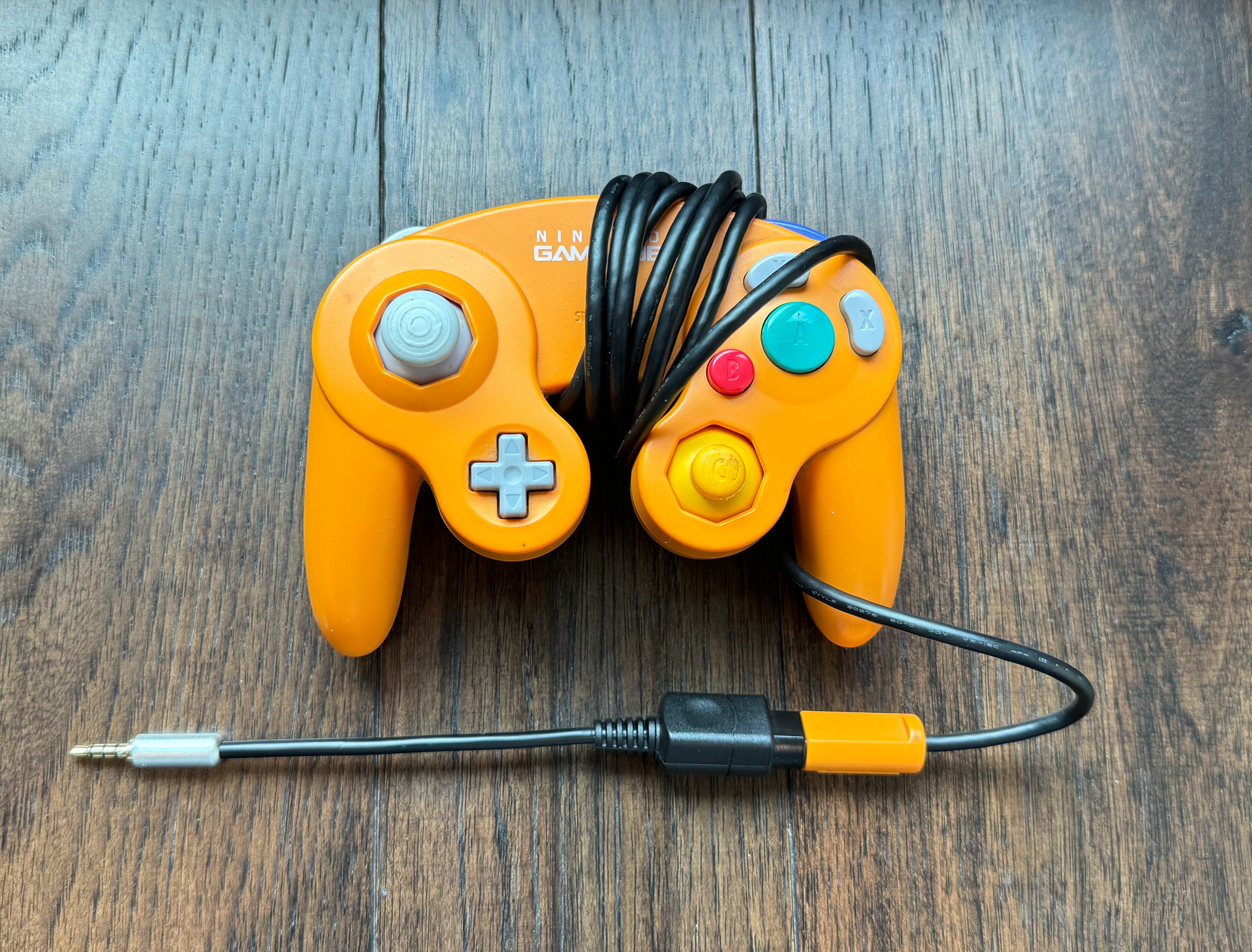
Since the GameCube controller connectors on the original Wii wouldn't fit cleanly on a build of this size, I use TRRS headphone connectors instead. This is the exact same approach used on the amazing GC Nano and in fact I made sure the dongles are pinout compatible!
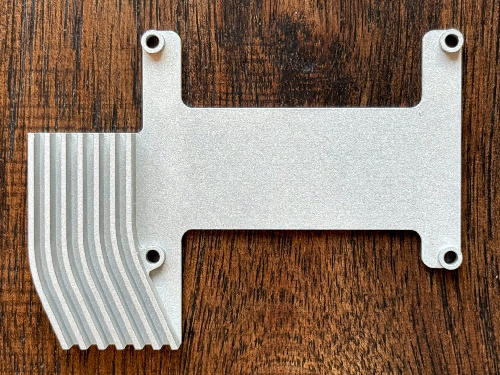
The final part of the "stack" is a custom heatsink which is designed to be as low profile as possible, while still providing adequate cooling for the Wii's CPU and GPU. The heatsink is designed to be machined from aluminum or copper, and incorporates mounting holes which align with those on the Wii motherboard.
I managed to find a tiny 5V blower fan (Pelonis AGB208N) which measures just 20x20x8mm and somehow puts out 0.84 CFM of air. This blows air through the heatsink fins, out the side of the case.
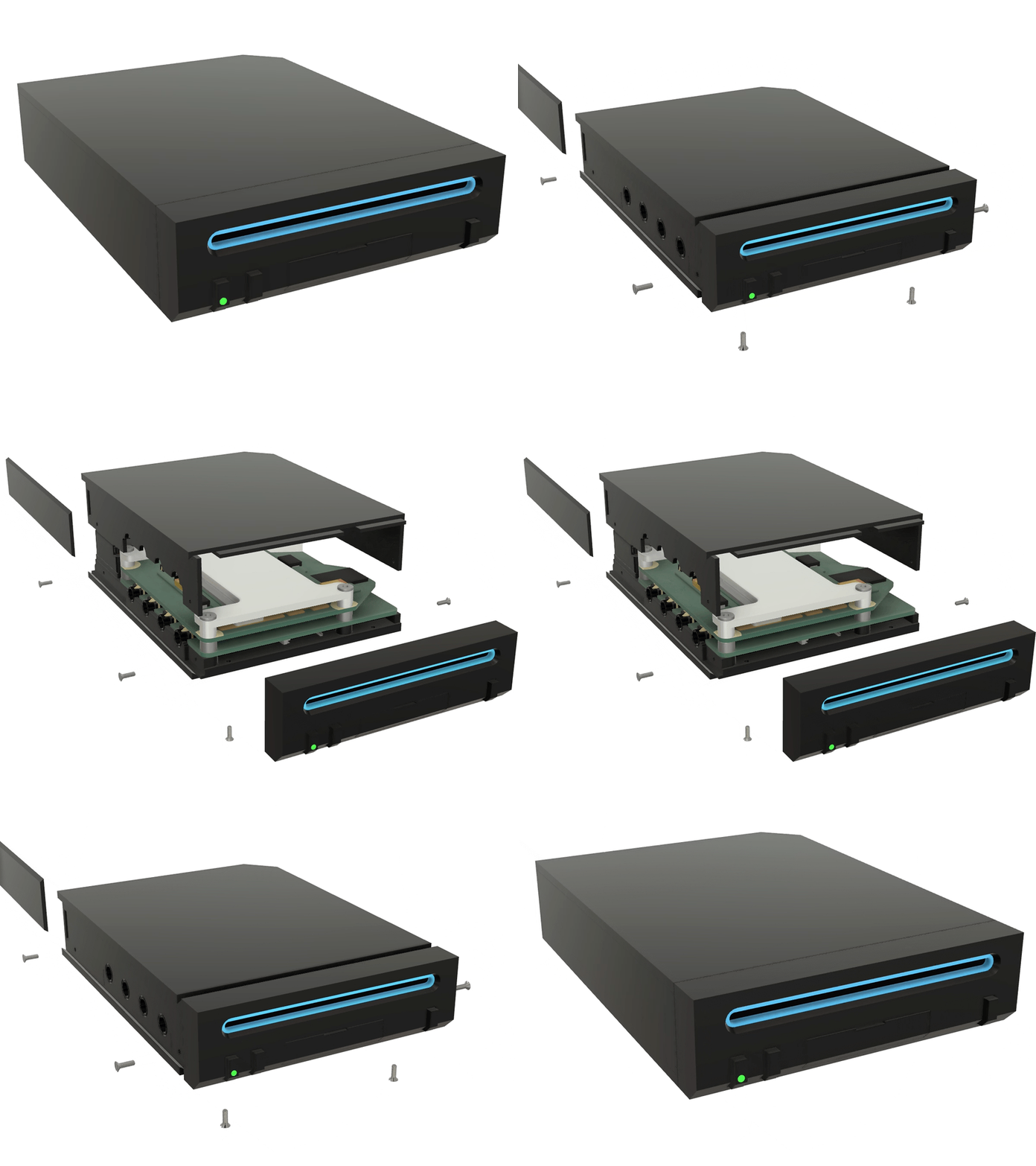
The stack is housed in a custom 3D printed case, secured with four M2.5 screws and spacers. The rest of case is assembled using self-tapping M1.2 screws. The screw locations and fan vents are positioned to match the original Wii case as closely as possible, to minimize visible screws.
You can access files on the SD card by connecting the console to a computer via USB, but I also included an access panel on the front of the case where the original Wii SD card slot is found. This panel is held in place by magnets and can be removed to access the SD card without opening the case. Shout out to Wesk for the magnet idea!
To keep the clean aesthetic of the original Wii I wanted to hide the GameCube controller ports behind a panel. I always hated the hinged design of the original, and it is quite difficult to replicate at this scale, so I redesigned this panel to be a sliding panel.
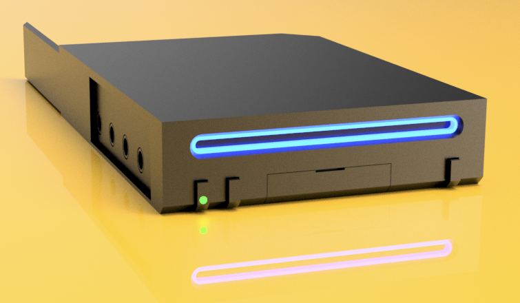
The Wii's iconic disc slot lights are recreated using a 1.5mm thick custom cut acrylic light diffuser, which is illuminated by two side-mounted addressable LEDs on the front panel board. The power, reset, and sync buttons are all also 3D printed, and the power button hosts a tiny light pipe to allow the power LED to shine through.
I FDM printed the case on a Voron 2.4 in ABS using a 0.4mm nozzle at 0.1mm layer height, but it should print fine in PLA or PETG on a well-tuned printer. At this scale, dimensional accuracy is important. In theory it should be possible to print this on an SLA printer, but I haven't tried it.
[!CAUTION] This is not a beginner project! This build requires performing a challenging motherboard trim, fine pitch soldering, and PCB assembly. If you are not comfortable with these tasks, I would recommend starting with a simpler project and working your way up - check out the BitBuilt forums for some awesome project worklogs.
SHUTDOWN via firstThis project would not be possible without the amazing BitBuilt community, I'm truly standing on the shoulders of giants here.
In particular, I'd like to thank:
Permissively released under the Solderpad Hardware License v2.1
| Qty | Value | Footprint | References |
|---|---|---|---|
| 5 | 1uF | Capacitor_SMD:C_0402_1005Metric | C9, C12, C14, C15, C16 |
| 4 | 0.1uF | Capacitor_SMD:C_0402_1005Metric | C10, C17, C19, C20 |
| 4 | 100K | Resistor_SMD:R_0402_1005Metric | R2, R4, R6, R8 |
| 4 | 10uF | Capacitor_SMD:C_0805_2012Metric | C2, C4, C6, C8 |
| 4 | 1uH | project-footprints:L_Vishay_IHLP-1212 | L1, L2, L3, L4 |
| 4 | 22uF | Capacitor_SMD:C_0805_2012Metric | C1, C3, C5, C7 |
| 4 | MountingHole_Pad | MountingHole:MountingHole_2.7mm_M2.5_ISO7380_Pad_TopBottom | H1, H2, H3, H4 |
| 4 | SJ-43504 | project-footprints:SJ-43504-SMT-TR | J1, J2, J3, J4 |
| 4 | TLV62585DRL | project-footprints:SOTFL50P160X60-6N | U1, U2, U3, U4 |
| 3 | 10K | Resistor_SMD:R_0402_1005Metric | R12, R13, R14 |
| 3 | 4.7uF | Capacitor_SMD:C_0402_1005Metric | C11, C13, C18 |
| 2 | 5.1K | Resistor_SMD:R_0402_1005Metric | R9, R10 |
| 1 | 2.2K | Resistor_SMD:R_0402_1005Metric | R11 |
| 1 | 200K | Resistor_SMD:R_0402_1005Metric | R5 |
| 1 | 453K | Resistor_SMD:R_0402_1005Metric | R7 |
| 1 | 5033981892 | project-footprints:503398-1892 | J11 |
| 1 | 5034800800 | project-footprints:5034800800 | J12 |
| 1 | 5034801400 | project-footprints:5034801400 | J6 |
| 1 | 5040500591 | project-footprints:5040500591 | J5 |
| 1 | 541020164 | project-footprints:Wii_Bluetooth_Module | J7 |
| 1 | 66.5K | Resistor_SMD:R_0402_1005Metric | R1 |
| 1 | 750 | Resistor_SMD:R_Array_Concave_4x0603 | RA1 |
| 1 | 92K | Resistor_SMD:R_0402_1005Metric | R3 |
| 1 | ATtiny1616-M | Package_DFN_QFN:VQFN-20-1EP_3x3mm_P0.4mm_EP1.7x1.7mm | U8 |
| 1 | AVE-HDMI Connector | project-footprints:5052781933 | J9 |
| 1 | AVR-UPDI-6 | project-footprints:UPDI Pads | J15 |
| 1 | BAT54GWJ | Diode_SMD:D_SOD-123 | D1 |
| 1 | DRDC3105F-7 | Package_TO_SOT_SMD:SOT-23 | U10 |
| 1 | GL835 | Package_DFN_QFN:QFN-24-1EP_4x4mm_P0.5mm_EP2.6x2.6mm | U6 |
| 1 | HDMI_C_1.4 | project-footprints:20139781 | J10 |
| 1 | JST-SH | project-footprints:JST_SH_SM02B-SRSS-TB_1x02-1MP_P1.00mm_Horizontal | J13 |
| 1 | MIC5504-3.3YM5 | Package_TO_SOT_SMD:SOT-23-5 | U7 |
| 1 | SiP32510 | Package_TO_SOT_SMD:TSOT-23-6 | U9 |
| 1 | T- | TestPoint:TestPoint_Pad_D1.0mm | TP1 |
| 1 | TMUXHS221NKGR | project-footprints:TMUXHS221NKGR | U5 |
| 1 | USB-C Connector | project-footprints:MOLEX_2171790001 | J8 |
It measures 62.1 × 83.8 mm and has 4 copper layers, 1.2 mm thick.
69 parts, built around the ATTINY1616-MN, TLV62585DRL, DRDC3105F-7 and MIC5504-3.3YM5-TR. The full list of its parts is on this page, with links to each part's symbol and footprint where PCBKit's library has them.
From the loopj/short-stack repository on GitHub, at the commit this page was made from: the board is main-board/KiCad/ss-main-board.kicad_pcb and its schematic front-panel/KiCad/ss-front-panel.kicad_sch. PCBKit opens the board in the browser, with nothing to install.
Its repository states no licence, so its author keeps all rights: ask loopj before reusing the design.
loopj/short-stack
World's Smallest Nintendo Wii, using a trimmed motherboard and custom stacked PCBs

MertX2/PowerStripHavoc
Its name is a combination of loopj's PowerStrip, which is the base of this project, and the Havoc weapon from Apex Legends.


taskx6004/limejig
Open-source LimeJig fixture firmware, host tools, KiCad source, and synthetic test examples

the78mole/jumpstarter-mono
This is a monorepo containing all jumpstarter tools and (hopefully) adds a standalone server soon.

trabem/home_sense_meteostation
Репозиторій автономної battery-powered метеостанції на ESP32-C3-WROOM-02. Містить firmware (ESP-IDF / FreeRTOS), KiCad-проєкти двох плат і матеріали фінальної презентації.

i2cjak/Chudx_Nano_100
a really cool macropad that's opensource btw
