
4 layers62.1 × 83.8 mm
Ss main board
loopj/short-stack
World's Smallest Nintendo Wii, using a trimmed motherboard and custom stacked PCBs
69 parts804

 nezumee/amber10
Personalized split keyboard based on Zebra experimentation
Amber is an open-source printed circuit board by nezumee, from the nezumee/amber repository on GitHub, published under the MIT licence. It is a 2-layer board of 118.9 × 112.3 mm with 50 parts on 46 nets, routed with 648 tracks and 73 vias.
It is built around the SJ-43504-SMT-TR. Its parts include 18 diodes, 17 switches, 6 connectors, 1 capacitor and 1 resistor. It belongs with the keyboards and input boards and the AVR (ATmega, ATtiny) boards of this library.
Personalized split keyboard based on Zebra experimentation.
This design was created with help of the https://github.com/mrzealot/ergogen tool that makes it easier to generate keyboard plates and PCBs.
Rough steps used:
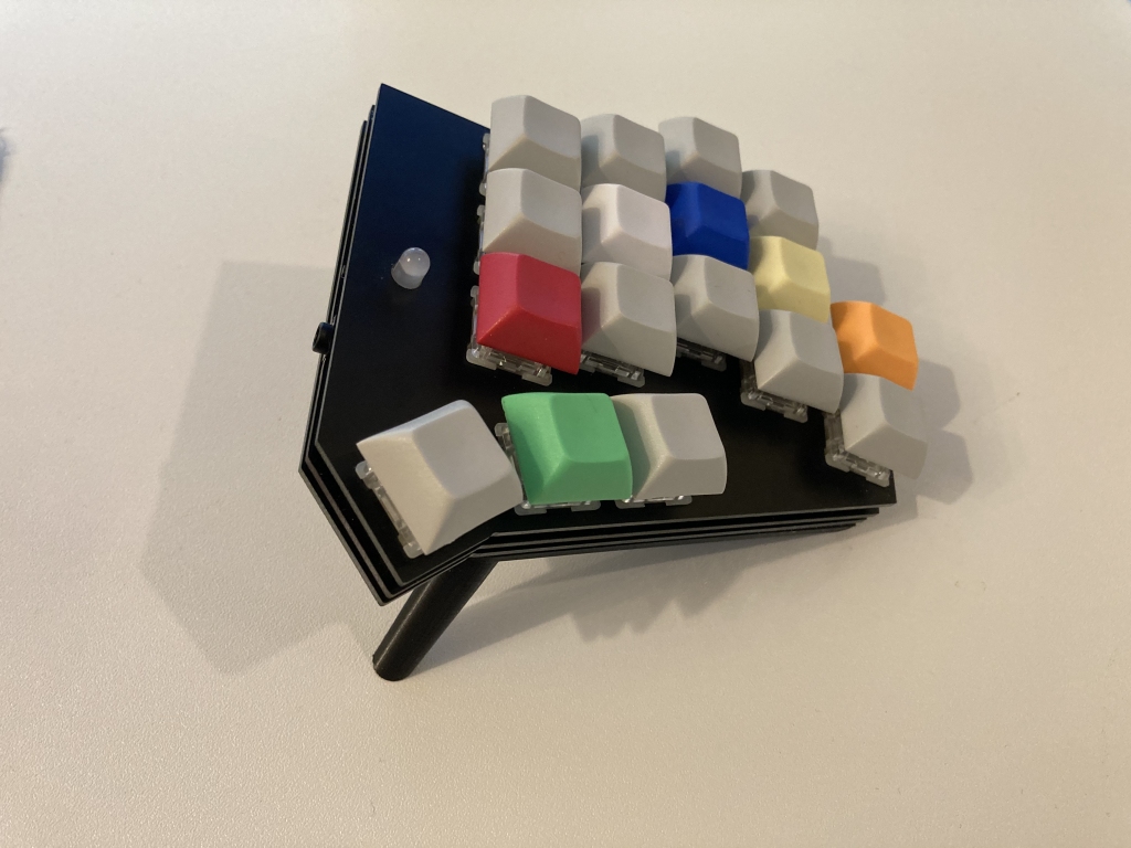
Many keyboards using ProMicro (like Corne) either have the ProMicro exposed, or use a small plate to cover it separately from the switch plate. While the tech prototype look of showing the MCU is nice, sometimes you want something cleaner looking, and also less prone to gathering visible dust. With this in mind, I decided to make the front plate that serves both as a plate for the switches and also covers all the components on the PCB. This led to a few challenges:
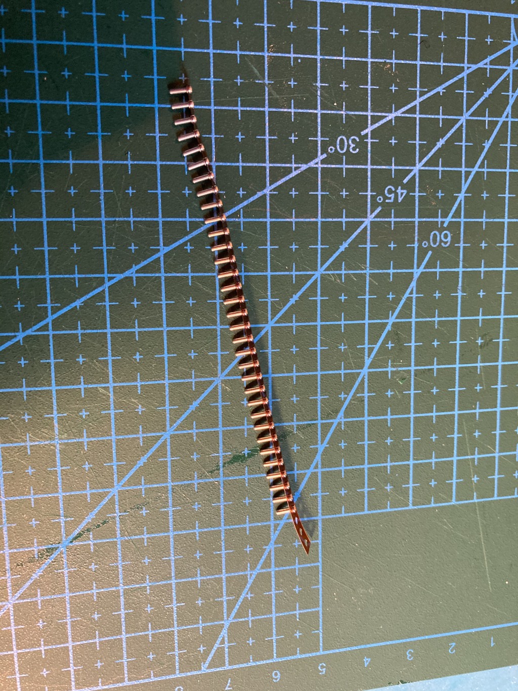
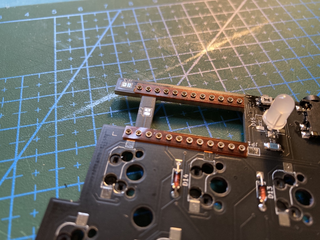
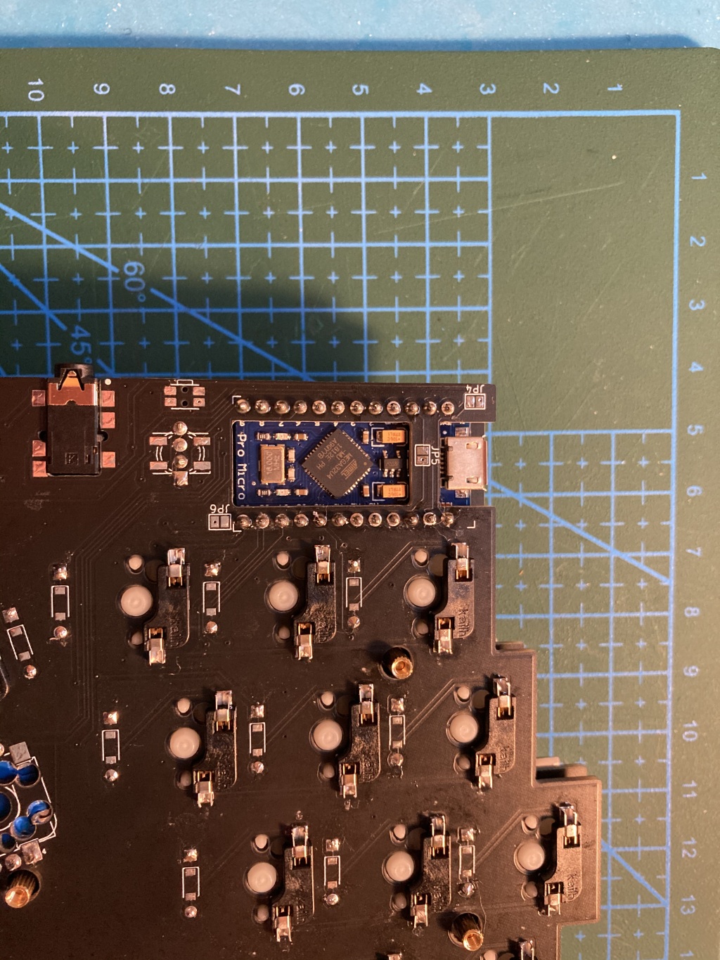
Fit a TRRS jack between the plates. The jack commonly used is even thicker than ProMicro with a socket. Luckily, it turned out there are special mid-mount jacks that mount into a cutout in the PCB: CUI Devices SJ-4350 series available on DigiKey, or PJ342C available on AliExpress (I got both; despite the differences in diagrams on seller sites, the ones I got look identical).
Fit a reset button between the plates. This was straightforward, there's a number of thin tactile buttons available. I picked a small switch with button on the side. It turned out to be difficult to press, but I feel it's not a big deal since I don't use it often. Reset command can be added somewhere in the layout if needed.
With this, everything fits between the plates comfortably:
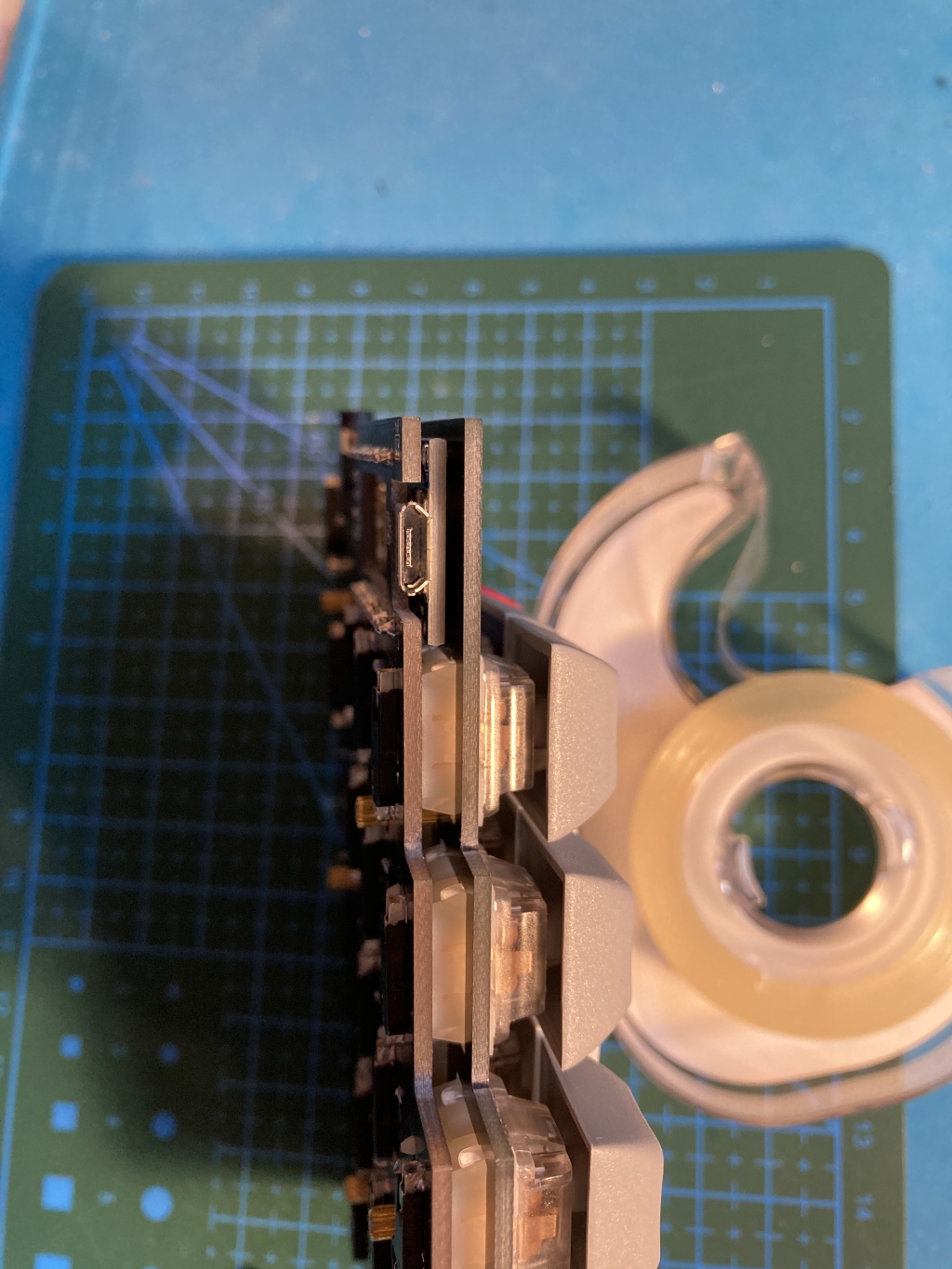
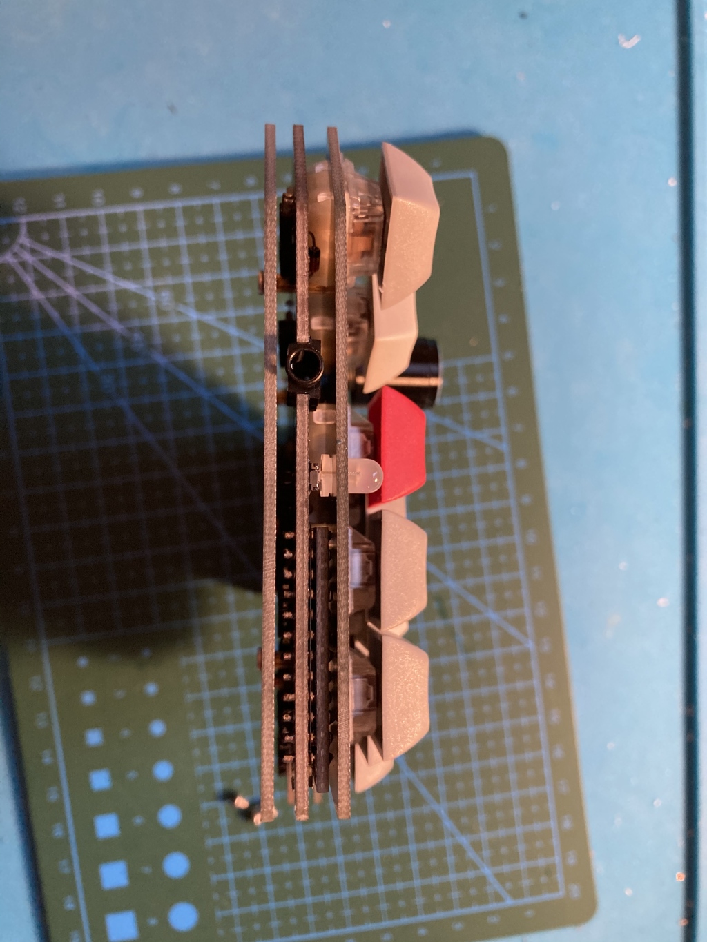
Of course, I waste all this effort by almost always using the keyboard with tented legs, attached using magnets: Things/Tented-base.stl.
| Qty | Value | Footprint | References |
|---|---|---|---|
| 16 | 1N4148 | amber:Diode_THT7.6_SOD123 | D1, D2, D3, D4, D5, D6, D7, D8, D9, D10, D11, D12, D13, D14, D16, D17 |
| 16 | SW_Push | amber:CherryMX_MidHeight_Hotswap | S1, S2, S3, S4, S5, S6, S7, S8, S9, S10, S11, S12, S13, S14, S16, S17 |
| 5 | kbd:M2_HOLE_v2 | P1, P2, P3, P4, P5 | |
| 3 | Jumper_2_Bridged | Jumper:SolderJumper-2_P1.3mm_Bridged_Pad1.0x1.5mm | JP1, JP2, JP3 |
| 3 | Jumper_2_Open | Jumper:SolderJumper-2_P1.3mm_Open_Pad1.0x1.5mm | JP4, JP5, JP6 |
| 1 | LED_BRCG | amber:LED_D5.0mm-4_RGB_Wide_Pins-dual | D15 |
| 1 | ProMicro_r | amber:ProMicro | C1 |
| 1 | R | Resistor_SMD:R_1206_3216Metric_Pad1.30x1.75mm_HandSolder | R1 |
| 1 | Rotary_Encoder_Switch | amber:Switch_MX2side_Encoder | S15 |
| 1 | SJ-43504-SMT-TR | amber:CUI_SJ-43504-SMT-TR-dual | J1 |
| 1 | SW_DIP_x01 | amber:SW_SPST_EVQP7C | B1 |
| 1 | YS-SK6812MINI-E | amber:LED_WS2812B-PLCC4-dual | LED1 |
It measures 118.9 × 112.3 mm and has 2 copper layers, 1.6 mm thick.
50 parts, built around the SJ-43504-SMT-TR. The full list of its parts is on this page, with links to each part's symbol and footprint where PCBKit's library has them.
From the nezumee/amber repository on GitHub, at the commit this page was made from: the board is amber.kicad_pcb. PCBKit opens the board in the browser, with nothing to install.
Its repository publishes it under the MIT licence: you may reuse it on that licence's terms (keep the author's notice, and for a copyleft licence share your changes alike).
loopj/short-stack
World's Smallest Nintendo Wii, using a trimmed motherboard and custom stacked PCBs


hackclub/OnBoard
💡 Join 1,000 teenagers and make your first PCB with a $100 grant!

dmcke5/NucDeck
The Open Source DIY Handheld Gaming PC!

