2 layers55 × 26.5 mm
 linuxboot/flashkeeper6
Documentation | Source | Join us on Matrix!
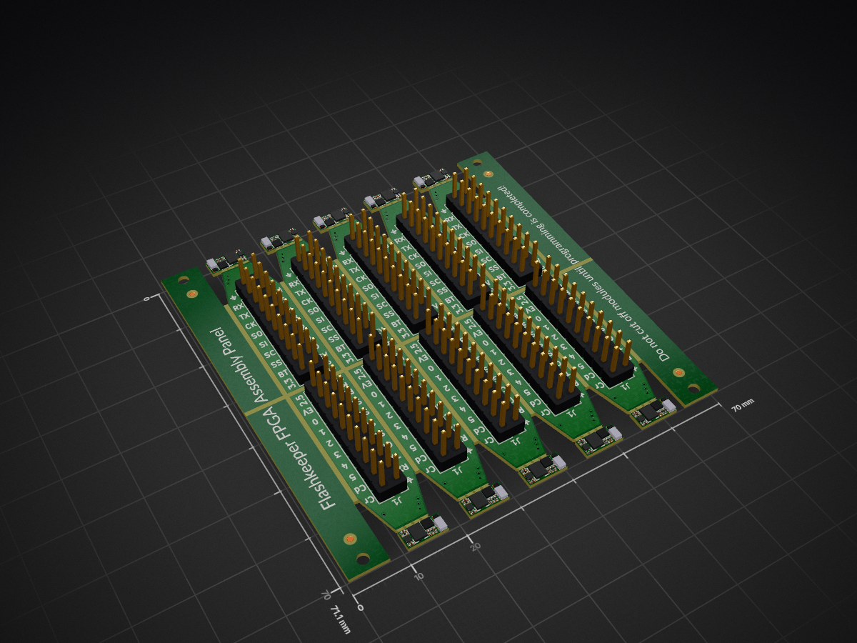
Fpga panelized is an open-source printed circuit board by linuxboot, from the linuxboot/flashkeeper repository on GitHub, published under the GPL-3.0 licence. It is a 6-layer board of 70 × 71.1 mm with 374 parts on 28 nets, routed with 3,640 tracks and 500 vias.
It is built around the ICE40UP5K-UWG30ITR, AT25DF041B-UUN-T and TPS7A2012PDQNR-TP. Its parts include 40 capacitors, 40 ICs, 20 resistors and 10 connectors. It belongs with the fPGA and programmable logic boards and the FPGA and CPLD boards of this library.


Documentation | Source | Join us on Matrix!
Flashkeeper is a family of open-hardware add-ons for standard SOIC-8 and WSON-8 SPI NOR flash chips (as are commonly used for firmware storage in PCs and other electronics), providing functionality for write-protection control, SPI bus breakout, flash device emulation, reprogramming, and state validation.
Flashkeeper development takes place on the 15h.org Git forge, and is mirrored to Github as a backup. If you wish to participate in Flashkeeper development on 15h.org infrastructure, please request an account in either the Flashkeeper room or the 15h.org room on Matrix. Issues may be opened on either 15h.org or Github.
For user information, please see the documentation. For hardware source files, see hw/.
The Flashkeeper project is supported by NLnet NGI Zero Core.
| Qty | Value | Footprint | References |
|---|---|---|---|
| 250 | ~ | flashkeeper:FPGACenterPad | TP1, TP1, TP1, TP1, TP1, TP1, TP1, TP1, TP1, TP1, TP10, TP10, TP10, TP10, TP10, TP10 +234 |
| 40 | 4.7 uF | flashkeeper:C_Smaller_0201 | C1, C1, C1, C1, C1, C1, C1, C1, C1, C1, C2, C2, C2, C2, C2, C2 +24 |
| 10 | 100 | flashkeeper:R_Smaller_0201 | R3, R3, R3, R3, R3, R3, R3, R3, R3, R3 |
| 10 | 10k | flashkeeper:R_Smaller_0201 | R1, R1, R1, R1, R1, R1, R1, R1, R1, R1 |
| 10 | 10k | flashkeeper:YC102 | RN1, RN1, RN1, RN1, RN1, RN1, RN1, RN1, RN1, RN1 |
| 10 | AT25DF041B-UUN-T | Package_CSP:WLCSP-8_1.58x1.63x0.35mm_Layout3x5_P0.35x0.4mm_Ball0.25mm_Pad0.25mm_NSMD | U3, U3, U3, U3, U3, U3, U3, U3, U3, U3 |
| 10 | Conn_02x09_Odd_Even | Connector_PinHeader_2.54mm:PinHeader_2x10_P2.54mm_Vertical | J1, J1, J1, J1, J1, J1, J1, J1, J1, J1 |
| 10 | ICE40UP5K-UWG30ITR | ICE40UP5K-UWG30ITR:BGA30N40P5X6_253X211X60N | U1, U1, U1, U1, U1, U1, U1, U1, U1, U1 |
| 10 | RV-3028-C8 | flashkeeper:RV-3028-C8 | U4, U4, U4, U4, U4, U4, U4, U4, U4, U4 |
| 10 | TPS7A2012PDQNR | Package_SON:Texas_X2SON-4_1x1mm_P0.65mm | U2, U2, U2, U2, U2, U2, U2, U2, U2, U2 |
The 370 most common of 374 parts.
It measures 70 × 71.1 mm and has 6 copper layers, 0.8 mm thick.
374 parts, built around the ICE40UP5K-UWG30ITR, AT25DF041B-UUN-T and TPS7A2012PDQNR-TP. The full list of its parts is on this page, with links to each part's symbol and footprint where PCBKit's library has them.
From the linuxboot/flashkeeper repository on GitHub, at the commit this page was made from: the board is hw/fpga/fpga_panelized.kicad_pcb and its schematic hw/adapter_soldered/breakout_wide/adapter_soldered.kicad_sch. PCBKit opens the board in the browser, with nothing to install.
Its repository publishes it under the GPL-3.0 licence: you may reuse it on that licence's terms (keep the author's notice, and for a copyleft licence share your changes alike).


AlexeyInwerp/BoardRipper
Web-based PCB boardview viewer for board-level repair. 14 formats: BVR1/3, BRD, BDV, BDV ASC, FZ, GenCAD, Mentor Neutral, XZZ, TVW, Allegro v15-v18, Altium, KiCad, EAGLE.


spacelab-ufsc/eps-re-hardware
Hardware project of the EPS-RE module


JulienKluge/Clock-odial
Clock-odial is a PCB featuring a ECP5 fpga for frequency/clock signal processing

nyuad-space/dumpling
Modular payload for high-speed logging and benchmarking of COTS sensors, enabling real-world performance data and open sharing.

embeddedci-com/pcb-trace-length-analyzer
Two of them, and the difference between them is the point.