4 layers60 × 130 mm
Parsnip
LimesKey/parsnip-node
A portable LoRa communicator. Custom 4-layer PCB (ESP32-S3 + E22P-915M30S LoRa + NEO-M9N GNSS), designed in KiCad for 915 MHz.
481 parts6

 LimesKey/parsnip-node6
A portable LoRa communicator. Custom 4-layer PCB (ESP32-S3 + E22P-915M30S LoRa + NEO-M9N GNSS), designed in KiCad for 915 MHz.
Selftest amp2 is an open-source printed circuit board by LimesKey, from the LimesKey/parsnip-node repository on GitHub. It is a 2-layer board of 30 × 20 mm with 9 parts on 5 nets, routed with 6 tracks and 0 vias.
Its parts include 3 ICs, 3 connectors and 1 capacitor. It belongs with the radio and wireless boards and the ESP32 boards of this library.
A battery-powered, portable Meshtastic/Meshcore node built around the ESP32-S3, an Ebyte E22P-915M30S LoRa front end, and a u-blox NEO-M9N GNSS receiver. Designed in KiCad, it targets 915 MHz operation in Canada under ISED RSS-247.
The goal is a self-contained LoRa node that pairs one of the longest range, best value LoRa modules, with an accurate GNSS reciever, running off two 21700 cells in series, to connect to other people on the LoRa mesh network community.

GNSS / active antenna |

LoRa front end |

Power rails |

Charger / BMS |

USB-C / PD |

Peripherals |
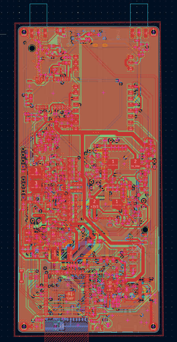
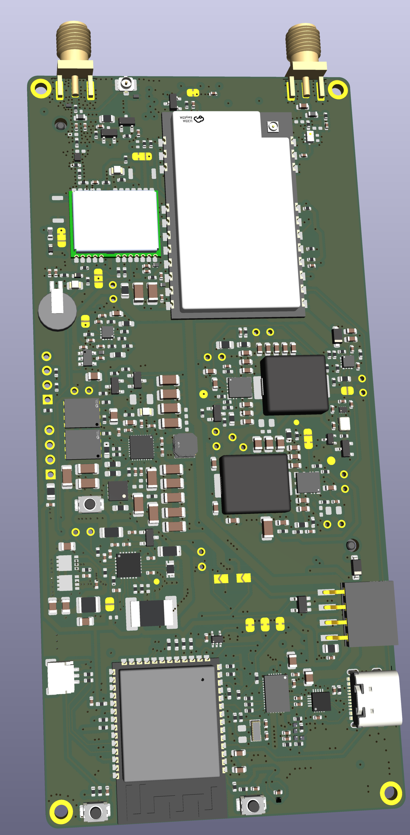
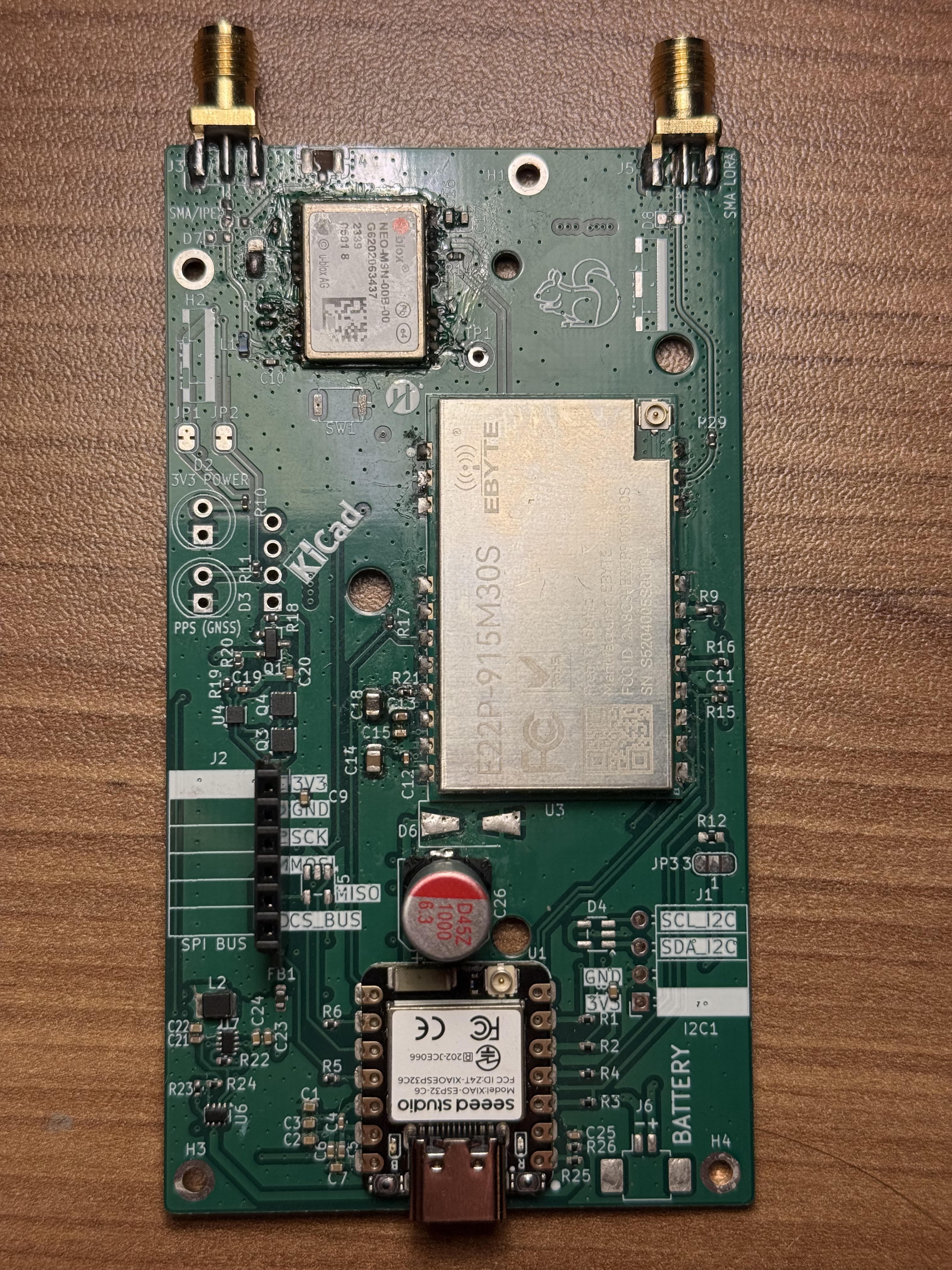
Assembled board |
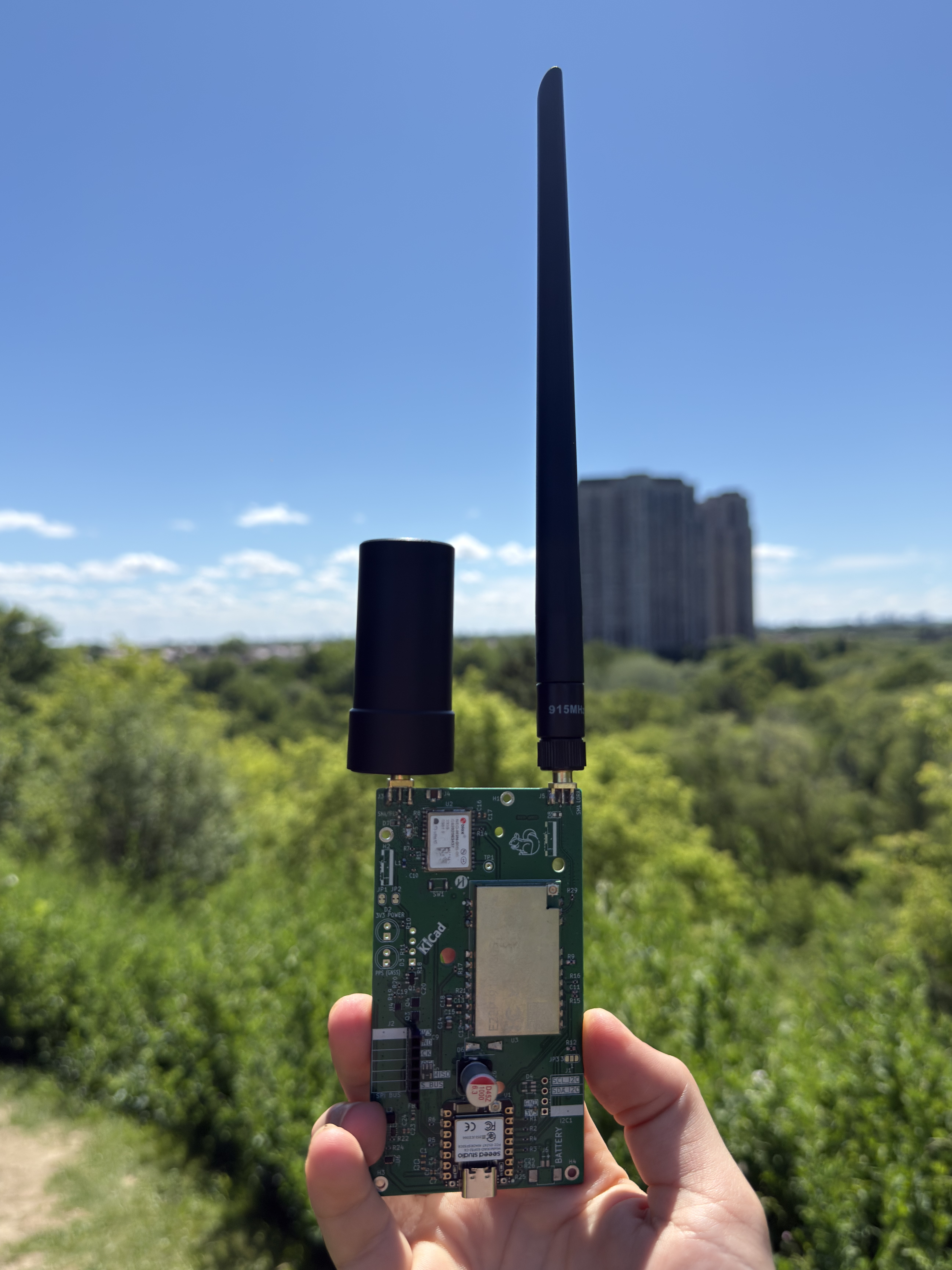
Outdoor testing |
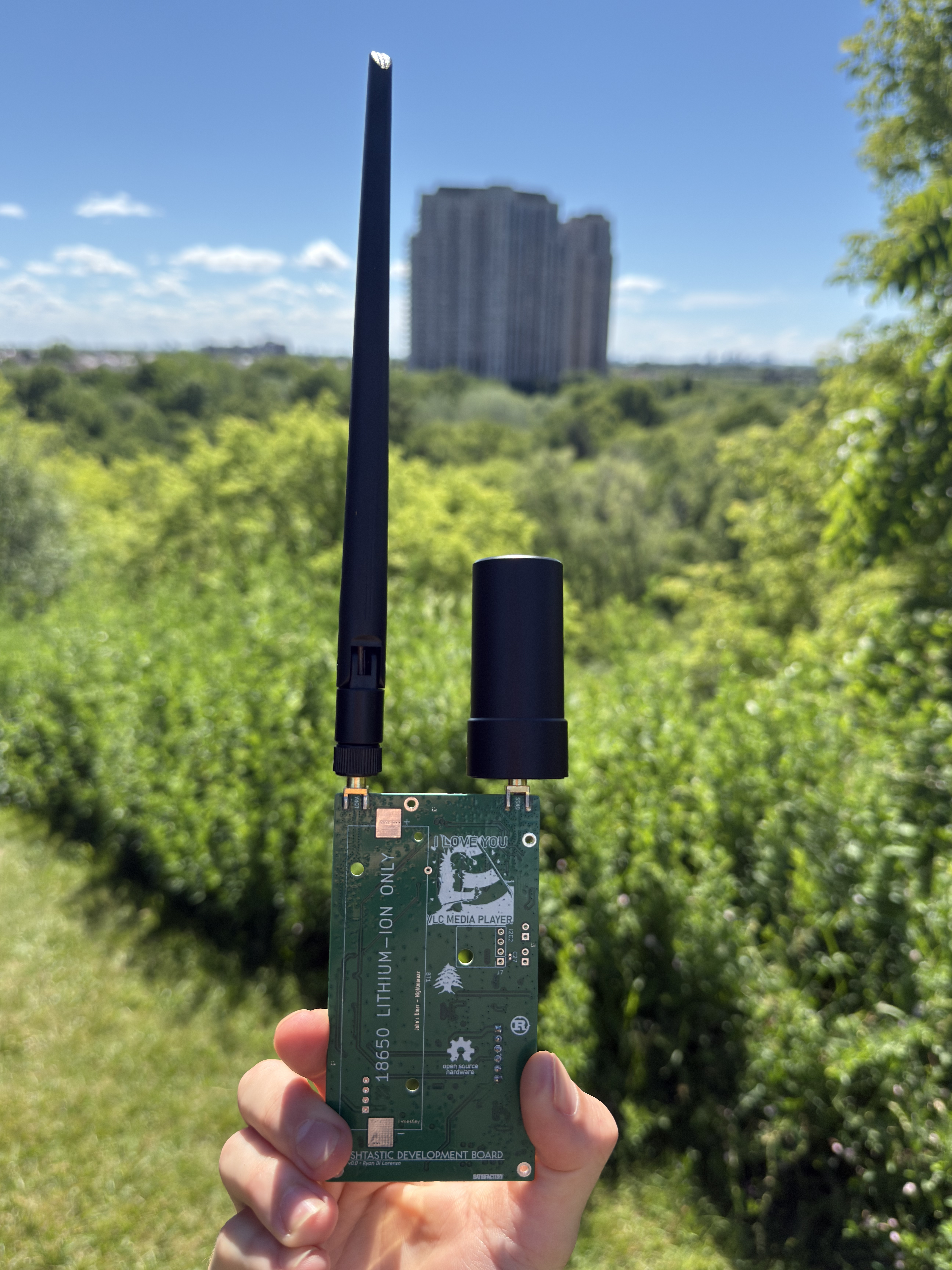
Outdoor testing, back |
| Part | Price |
|---|---|
| JLCPCB PCB w/ Assembly (to-be changed BOM) | $1098.04 CAD (est) |
| 21700 Cells 18650batterystore.com | $40 CAD |
| 3.7" E-Ink AliExpress | 24$ CAD |
JLC04161H-7628 stackup, 2 oz copper outer, 2 oz copper innerHost: ESP32-S3-WROOM-1-N16R8 (U1). GPIO numbers are ESP32-S3 GPIO, not module pins.
| Signal | GPIO |
|---|---|
| NSS | 10 |
| SCK | 12 |
| MOSI | 11 |
| MISO | 13 |
| BUSY | 14 |
| DIO1 | 4 |
| NRST | 40 |
| EN | 41 |
| Signal | GPIO |
|---|---|
| TXD | 1 |
| RXD | 2 |
| TIMEPULSE | 3 |
| EXTINT | 48 |
| SDA | 8 |
| SCL | 9 |
| Function | GPIO |
|---|---|
| I2C SDA | 8 |
| I2C SCL | 9 |
| I2C IRQ | 7 |
| E-Ink BUSY | 5 |
| E-Ink RESET | 6 |
| E-Ink D/C | 18 |
| E-Ink CS | 17 |
| Bus CS | 38 |
| USB D- / D+ | 19 / 20 |
| UART0 TX / RX | 43 / 44 |
| RTC 32 kHz xtal | 15 / 16 |
| BOOT | 0 |
| eFuse PG | 39 / 42 |
| EMI osc gate | 47 |
| Level shifter | 46 |
| Load switch | 21 |
| PSRAM (reserved) | 35 / 36 / 37 |
| VDD_SPI (reserved) | 45 |
Firmware is a Meshtastic fork tracked as the firmware submodule (LimesKey/firmware). Development uses VS Code with the pioarduino extension, which Meshtastic pins for ESP32-C6 / Arduino-ESP32 3.x support. A device variant declares the pin map above and the PA control lines so TX actually keys up. Unfortunately there are some extensive changes to the Meshtastic firmware in order to incorporate a SPI GNSS module, as this is not natively supported by Meshtastic.
git clone --recurse-submodules https://github.com/LimesKey/parsnip-node.git| Qty | Value | Footprint | References |
|---|---|---|---|
| 3 | HDR | test:FP | J1, J2, J3 |
| 2 | NTC10K | test:FP | TH1, TH2 |
| 1 | 10uF | test:FP | C1 |
| 1 | COVERED | test:FP | U2 |
| 1 | FINEPITCH | test:FP | U1 |
| 1 | GAPPED | test:FP | U3 |
LimesKey/parsnip-node
A portable LoRa communicator. Custom 4-layer PCB (ESP32-S3 + E22P-915M30S LoRa + NEO-M9N GNSS), designed in KiCad for 915 MHz.

LimesKey/parsnip-node
A portable LoRa communicator. Custom 4-layer PCB (ESP32-S3 + E22P-915M30S LoRa + NEO-M9N GNSS), designed in KiCad for 915 MHz.


FrameworkComputer/ExpansionCards
Reference designs and documentation to create Expansion Cards for the Framework Laptop

VoronDesign/Voron-Hardware
Cool Hardware designed by the Voron Design group

hackclub/OnBoard
💡 Join 1,000 teenagers and make your first PCB with a $100 grant!


adamws/kicad-kbplacer
KiCad plugin for automatic keyboard's key placement and routing
It measures 30 × 20 mm and has 2 copper layers, 1.6 mm thick.
9 parts. The full list of its parts is on this page, with links to each part's symbol and footprint where PCBKit's library has them.
From the LimesKey/parsnip-node repository on GitHub, at the commit this page was made from: the board is code/claude/kicad-review/references/selftest_amp2.kicad_pcb and its schematic block_diagram.kicad_sch. PCBKit opens the board in the browser, with nothing to install.
Its repository states no licence, so its author keeps all rights: ask LimesKey before reusing the design.