
2 layers50 × 50 mm
T85-with driver and poe
cnlohr/ethertiny
A firmware-only half-duplex 10Base-T implementation for AVRs
41 parts133

 lily-osp/quad-tic-timer
Four synchronized phase-accurate pulse outputs from one pot (ATtiny85 firmware + 30x30mm KiCad 9 PCB)
Quad tic timer is an open-source printed circuit board by lily-osp, from the lily-osp/quad-tic-timer repository on GitHub. It is a 2-layer board of 30 × 30 mm with 17 parts on 14 nets, routed with 88 tracks and 10 vias.
It is built around the ATTINY85-15M. Its parts include 5 resistors, 4 diodes, 2 capacitors and 1 IC. It belongs with the AVR (ATmega, ATtiny) boards of this library.
A 30x30mm 2-layer KiCad 9 development board for the Quad-Tic-Timer firmware. Driven by an Atmel ATtiny85-20SU, it provides four synchronized phase-accurate pulse outputs scaled exponentially by a single precision 10-turn control pot.
Designed and verified using the pcb skill with full KiCad 9 headless tooling and production-ready JLCPCB fabrication deliverables.
| Top Side (Components & Telemetry) | Bottom Side (Ground Plane & Labeling) |
|---|---|
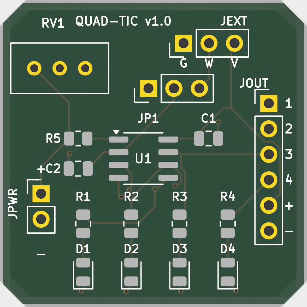 | 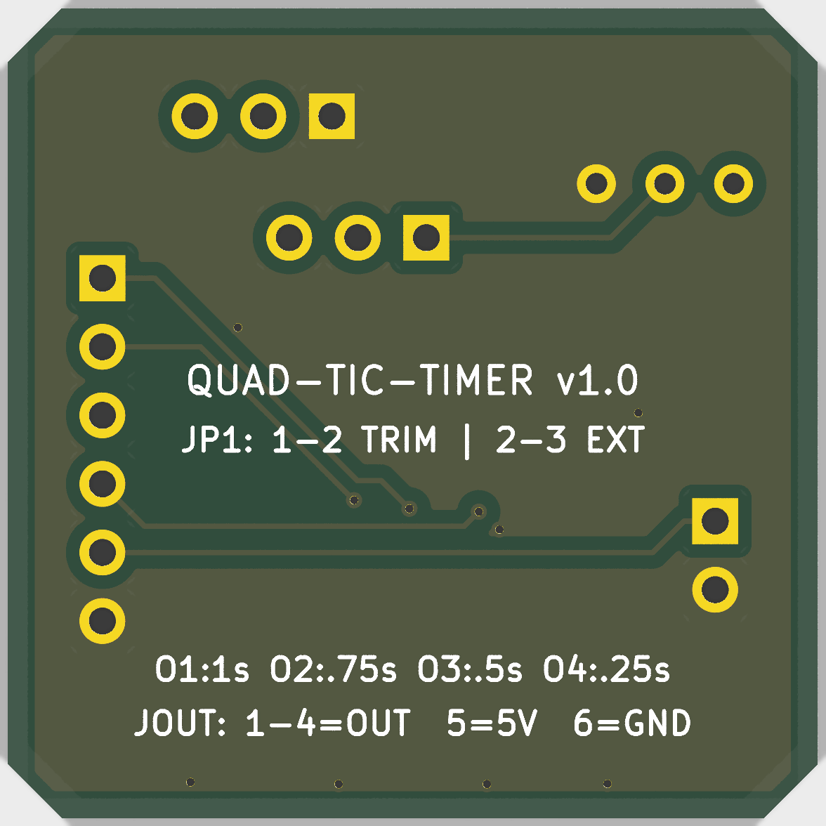 |
O1 (PB0 / Pin 5): 1.00 s/tic nominal (0.20 s – 5.00 s range)O2 (PB1 / Pin 6): 0.75 s/tic nominal (0.15 s – 3.75 s range)O3 (PB2 / Pin 7): 0.50 s/tic nominal (0.10 s – 2.50 s range)O4 (PB4 / Pin 3): 0.25 s/tic nominal (0.05 s – 1.25 s range)RV1).JEXT) for panel-mount 10-turn pots (Bourns 3590S).JP1). Jumper pins 1-2 for onboard trimmer, 2-3 for external pot.C1 (100nF 0805): Dedicated VCC decoupling placed within 2 mm of U1 pin 8.C2 (10nF 0805): Low-pass noise filter on ADC3 wiper input (U1 pin 2).R5 (10k 0805): Pull-up on RESET (pin 1) keeping reset line high while leaving it ISP-programmable.JPWR (1x02): 5V DC input.D1–D4) driven through 1kΩ ballast resistors (R1–R4) indicating pulse ticks on each channel.JOUT (1x06 2.54mm header): Exposes O1, O2, O3, O4, VCC, and GND.B.Cu).quad-tic-timer/pcb/
├── README.md # Comprehensive technical hardware documentation
├── fp-info-cache # KiCad footprint library cache
├── quad-tic-timer.kicad_pro # KiCad 9 project file
├── quad-tic-timer.kicad_prl # KiCad 9 local settings file
├── quad-tic-timer.kicad_sch # KiCad 9 complete schematic with embedded symbols
├── quad-tic-timer.kicad_pcb # KiCad 9 fully routed board (0 DRC, 0 unconnected)
├── quad-tic-timer-drc.rpt # Official KiCad DRC report (0 errors, 0 warnings)
├── quad-tic-timer-erc.rpt # Official KiCad ERC report (0 errors, 0 warnings)
└── jlcpcb_production/ # Turn-key manufacturing archive
├── quad-tic-timer_gerber_jlcpcb.zip # RS-274X Gerbers + Excellon NC drills
├── quad-tic-timer_bom_jlcpcb.csv # Bill of Materials formatted for JLCPCB
├── quad-tic-timer_cpl_jlcpcb.csv # Pick-and-place centroid coordinate file
├── quad-tic-timer_render_top.png # Photorealistic 3D top render
└── quad-tic-timer_render_bottom.png # Photorealistic 3D bottom render| Designator | Description | Footprint | LCSC Part # | Qty |
|---|---|---|---|---|
| U1 | ATtiny85-20SU 8-bit AVR Microcontroller | SOIC-8_3.9x4.9mm_P1.27mm | C44533 | 1 |
| RV1 | 10k Precision Multi-turn Trimpot | Bourns_3296W_Vertical | C180126 | 1 |
| C1 | 100nF 50V Ceramic Capacitor | C_0805_2012Metric | C49678 | 1 |
| C2 | 10nF 50V Ceramic Capacitor | C_0805_2012Metric | C1710 | 1 |
| R5 | 10kΩ 1% 1/8W Pullup Resistor | R_0805_2012Metric | C17414 | 1 |
| R1–R4 | 1kΩ 1% 1/8W LED Current-Limiters | R_0805_2012Metric | C17513 | 4 |
| D1–D4 | Green LED Indicators | LED_0805_2012Metric | C2297 | 4 |
| JPWR | 1x02 2.54mm Pin Header (Power In) | PinHeader_1x02_P2.54mm_Vertical | C2241 | 1 |
| JP1 | 1x03 2.54mm Pin Header (Pot Select) | PinHeader_1x03_P2.54mm_Vertical | C2242 | 1 |
| JEXT | 1x03 2.54mm Pin Header (Ext Pot) | PinHeader_1x03_P2.54mm_Vertical | C2242 | 1 |
| JOUT | 1x06 2.54mm Pin Header (Signal Out) | PinHeader_1x06_P2.54mm_Vertical | C2245 | 1 |
quad-tic-timer-erc.rpt: 0 errors, 0 warningsquad-tic-timer-drc.rpt: 0 errors, 0 warnings, 0 unconnected itemsEdge_Cuts (.gm1)quad-tic-timer_gerber_jlcpcb.zip ready for one-click upload.| Qty | Value | Footprint | References |
|---|---|---|---|
| 4 | 1k | R_0805_2012Metric | R1, R2, R3, R4 |
| 1 | 100n | C_0805_2012Metric | C1 |
| 1 | 10k | Potentiometer_Bourns_3296W_Vertical | RV1 |
| 1 | 10k | R_0805_2012Metric | R5 |
| 1 | 10n | C_0805_2012Metric | C2 |
| 1 | ATtiny85 | SOIC-8_3.9x4.9mm_P1.27mm | U1 |
| 1 | EXT-POT | PinHeader_1x03_P2.54mm_Vertical | JEXT |
| 1 | O1 | LED_0805_2012Metric | D1 |
| 1 | O2 | LED_0805_2012Metric | D2 |
| 1 | O3 | LED_0805_2012Metric | D3 |
| 1 | O4 | LED_0805_2012Metric | D4 |
| 1 | OUT | PinHeader_1x06_P2.54mm_Vertical | JOUT |
| 1 | POT-SEL | PinHeader_1x03_P2.54mm_Vertical | JP1 |
| 1 | PWR | PinHeader_1x02_P2.54mm_Vertical | JPWR |
It measures 30 × 30 mm and has 2 copper layers, 1.6 mm thick.
17 parts, built around the ATTINY85-15M. The full list of its parts is on this page, with links to each part's symbol and footprint where PCBKit's library has them.
From the lily-osp/quad-tic-timer repository on GitHub, at the commit this page was made from: the board is pcb/quad-tic-timer.kicad_pcb and its schematic pcb/quad-tic-timer.kicad_sch. PCBKit opens the board in the browser, with nothing to install.
Its repository states no licence, so its author keeps all rights: ask lily-osp before reusing the design.
cnlohr/ethertiny
A firmware-only half-duplex 10Base-T implementation for AVRs


Guiimartinho/routeai
LLM-Powered Electronic Design Automation Platform for PCB Design

rallekralle11/Tinyreflow
Inspired by afterearthltd's reflow plate, but using fewer and simpler components.

aleh/MIDIMonkey
Listens to MIDI messages on one pin and triggers drums on the others
