4 layers475.6 × 317.7 mm
OPSpec v0.0.2
lepton-7/Open-Plate-Spectrophotometer
An open-source project to build a 96-well spectrophotometer operating at 620nm. Designed from the ground-up focusing on robust electronic design.
153 partsGPL-3.0

 lepton-7/Open-Plate-Spectrophotometer
An open-source project to build a 96-well spectrophotometer operating at 620nm. Designed from the ground-up focusing on robust electronic design.
OPSpec v0.1.0 is an open-source printed circuit board by lepton-7, from the lepton-7/Open-Plate-Spectrophotometer repository on GitHub, published under the GPL-3.0 licence. It is a 4-layer board of 429.6 × 293.4 mm with 661 parts on 344 nets, routed with 1,185 tracks and 1,361 vias.
It is built around the ADS7828E, AP63205WU and MAX4206ETE+T, with the TAR5S50TE85LF, GR JTLPS1.23-G7H4-45-1-150-R33 and S16392-01CT among its other parts. Its parts include 227 resistors, 174 capacitors, 96 diodes, 38 transistors and 9 ICs.


An open-source project to build a 96-well spectrophotometer operating at 620nm. Designed from the ground-up focusing on robust electronic design. Funded by the think[box] Student Project Fund for the 2022-2023 academic year.
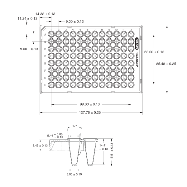
This project was born out of an appreciation for Cerillo's portable microplate reader and the arrogant desire to open-source it by recreating what they made on my own. I designed a limited test prototype during the summer (I think sometime in July?) before the school year restarted to see what is required to realise the idea of a small form-factor, portable plate reader.
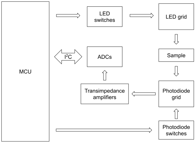
The idea is simple: control 96-element grids of LEDs and light sensors to address individual wells in a plate, convert the signal from the light sensor into something machine parsable, then finally do some ✨math✨ to get an optical density value for each well.
I decided to not build a full 96-capable prototype. Instead, I opted to test all the relevant units I needed on a smaller scale. The result was a prototype with all 8 rows (A-H) but only two columns.
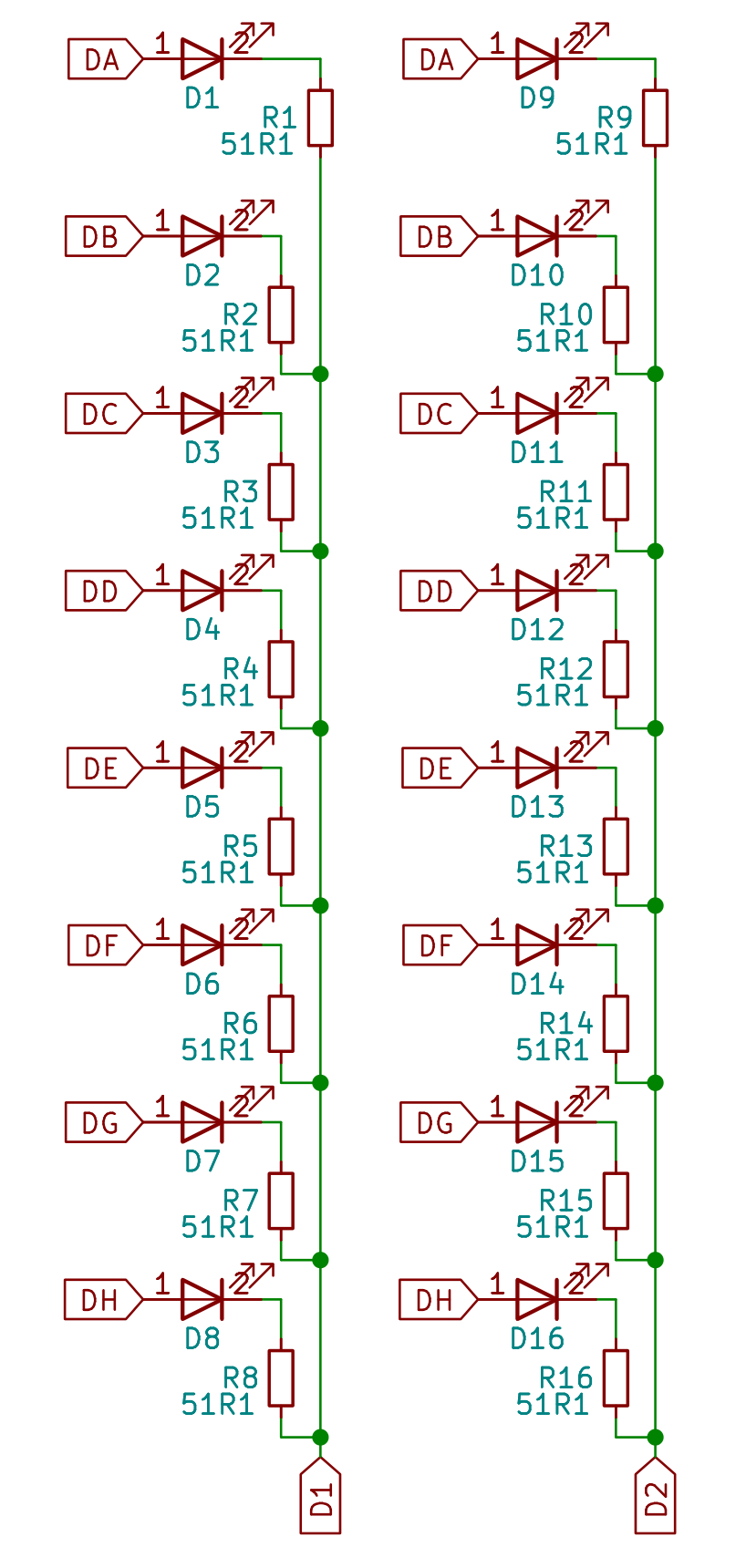 Independent control of each element is easily achieved by connecting the grid high and low sides to control MOSFETs:
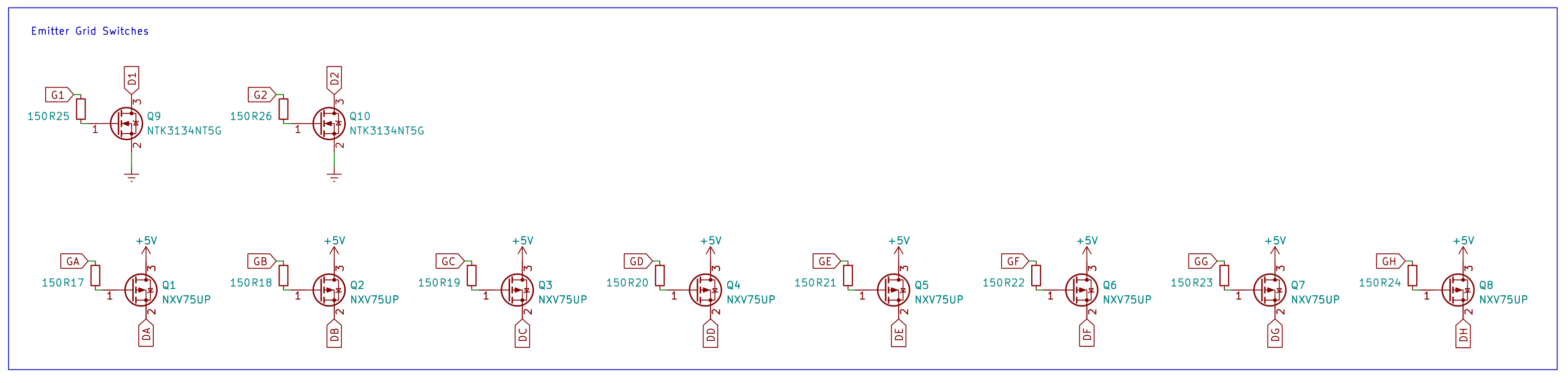 Each row was connected to +5V via p-ch FETs (yes i know, they're wired incorrectly) and each column was connected to GND via n-ch FETs. Each FET gate is assigned its own pin on the MCU to independently control individual elements.
A similar idea is used for switching inputs from specific photodiode elements.
The hard bit for a device like this taking light that passes through the sample wells and converting that into a digital signal. Initially, I planned on using phototransistors to transform a change in incident light intensity into a change in current. But these devices are pretty imprecise and do not have the best linearity. To make phototransistors work, I would have needed to do some really careful biasing -- something I did not think I needed.
The alternative was to use photodiodes. These are a bit better in the sense that they would have required a lot fewer supporting components. They also have pretty nice characteristics:
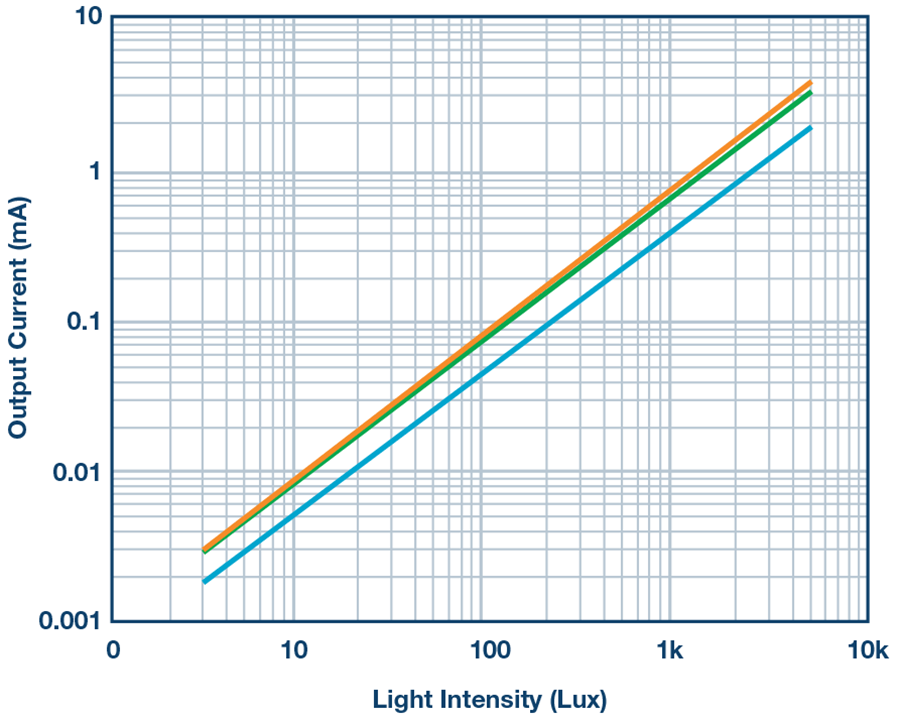 Plot from Analog ADI
These devices are pretty much linear in their response to incident light intensity: A 10x increase in incident intensity results in a 10x increase in reverse current.
Converting current going through a photodiode into digital information is a two-step process. This is nothing new; the typical strategy is to use a transimpedance amplifier to convert transform a current signal into a voltage signal followed by an ADC that can convert the voltage signal into a digital value:
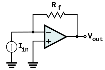 TIA diagram from wikimedia commons.
The transfer function is also pretty simple for a TIA: $$ V_{out} = -I_{in}R_f $$
This is implemented as:
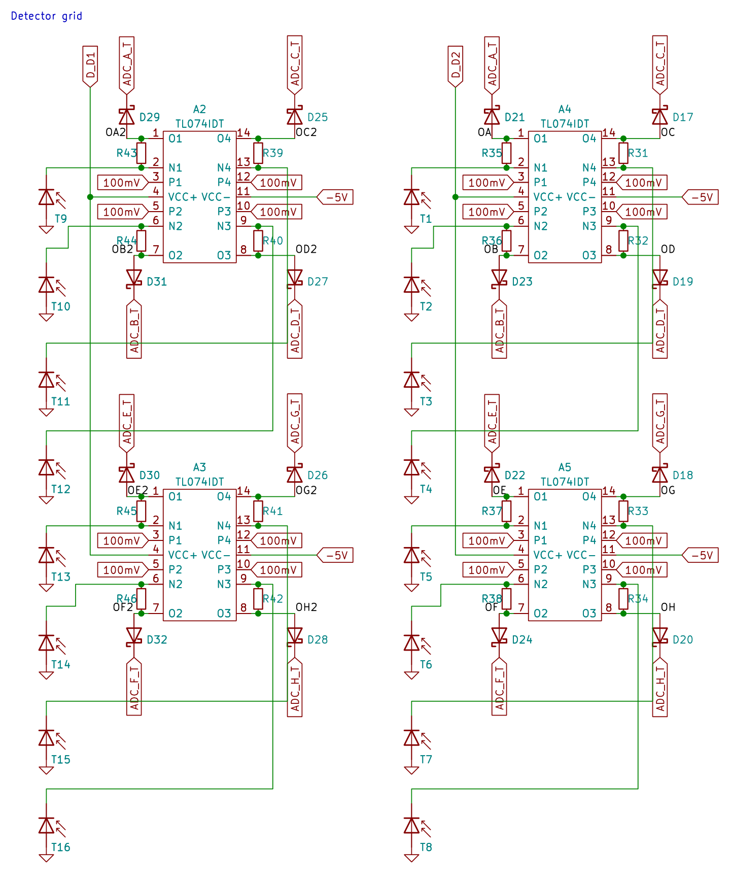
The principle is the same, just compressed a little. The current source is replaced by the photodiode, mulit-channel opamps are used to save space, and $V_{out}$ passes through a standard Schottky diode before being connected to the ADC inputs.
I used an 8ch ADC to independently connect each row for pseudo-switching of the detector outputs. High-side p-ch FET switches control Vcc for the TIAs.
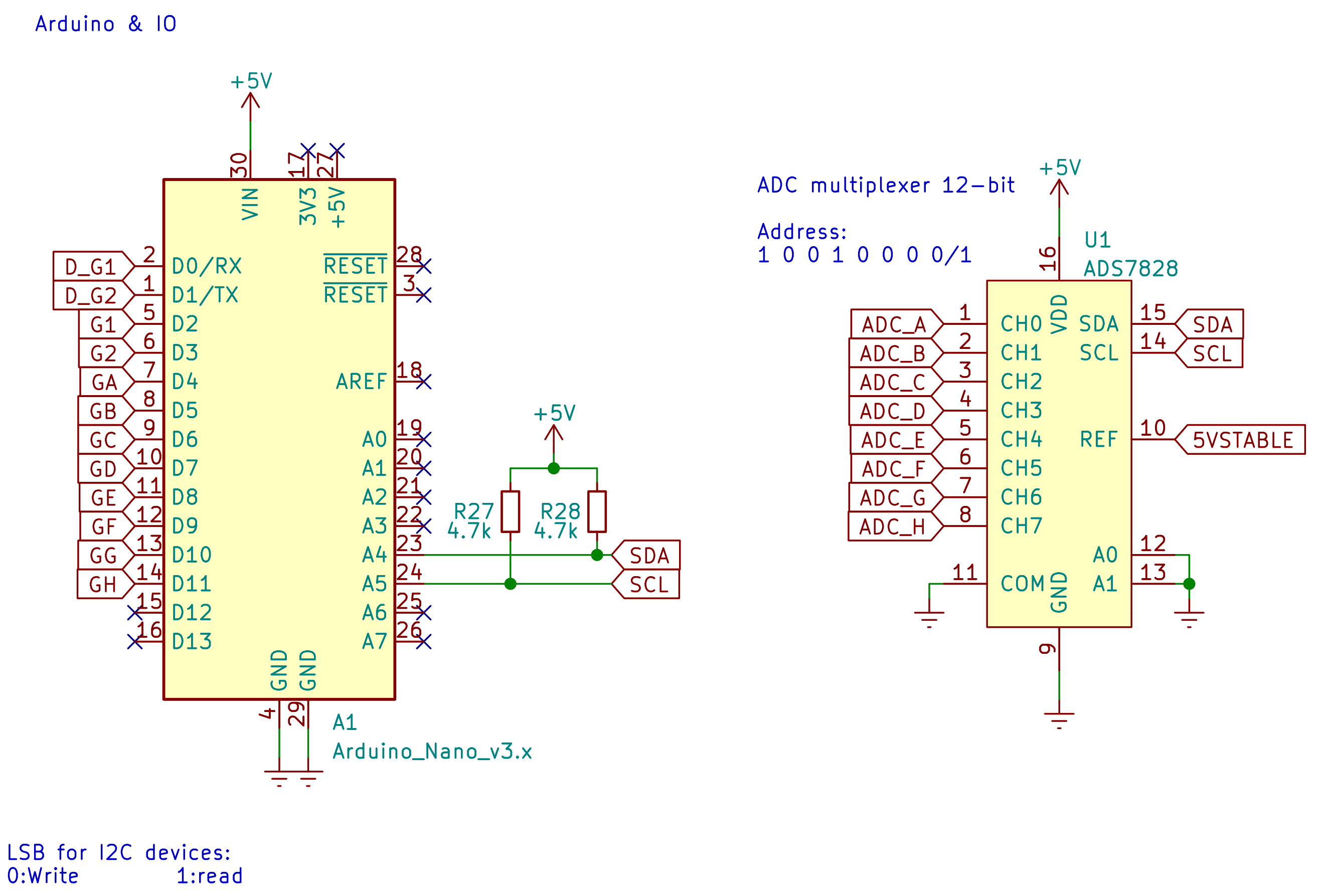
The 12-bit ADC converts output voltage into a digital signal referenced to a stable 5V signal generated by a voltage reference amplified by a low-noise voltage follower:
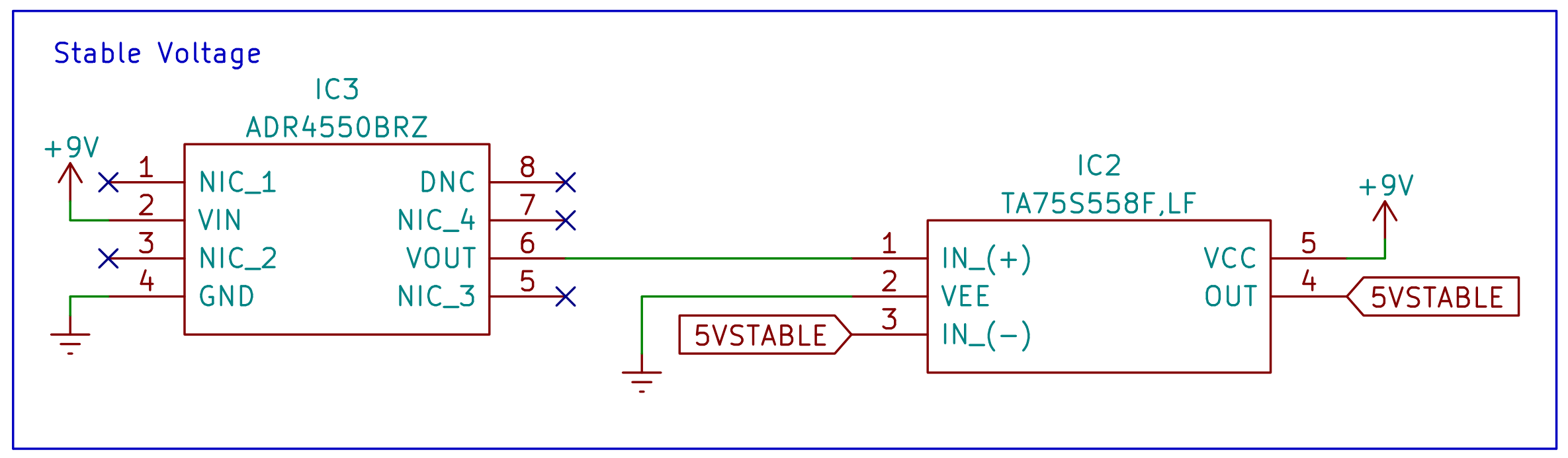
The MCU, an arduino nano, communicates with the ADC over I2C.
| Qty | Value | Footprint | References |
|---|---|---|---|
| 101 | 1u | Capacitor_SMD:C_0603_1608Metric | C1, C2, C10, C11, C12, C13, C14, C15, C16, C17, C18, C19, C100, C105, C154, C174 +85 |
| 96 | 51R1 | Resistor_SMD:R_0603_1608Metric | R1, R2, R10, R11, R12, R13, R14, R15, R16, R17, R18, R19, R20, R21, R22, R23 +80 |
| 96 | GR_JTLPS1.23-G7H4-45-1-150-R33 | SamacSys_Parts:GRJTLPS123G7H4451150R33 | D1, D2, D10, D11, D12, D13, D14, D15, D16, D17, D18, D19, D20, D21, D22, D23 +80 |
| 96 | S16392-01CT | Diode_SMD:S16392-01CT | T1, T2, T10, T11, T12, T13, T14, T15, T16, T17, T18, T19, T20, T21, T22, T23 +80 |
| 40 | 100nF | Capacitor_SMD:C_0603_1608Metric | C103, C106, C107, C108, C109, C110, C111, C112, C113, C114, C115, C116, C117, C118, C119, C120 +24 |
| 32 | 100k | Resistor_SMD:R_0603_1608Metric | R101, R103, R105, R107, R109, R111, R113, R115, R117, R119, R129, R130, R131, R132, R133, R134 +16 |
| 32 | 150 | Resistor_SMD:R_0603_1608Metric | R100, R102, R104, R106, R108, R110, R112, R114, R116, R118, R120, R121, R122, R123, R124, R125 +16 |
| 27 | 10k | Resistor_SMD:R_0603_1608Metric | R137, R138, R173, R174, R175, R176, R177, R178, R179, R180, R211, R212, R213, R214, R215, R216 +11 |
| 20 | NXV75UP | Package_TO_SOT_SMD:SOT-23 | Q13, Q14, Q15, Q16, Q17, Q18, Q19, Q20, Q21, Q22, Q23, Q24, Q25, Q26, Q27, Q28 +4 |
| 16 | 100 | Resistor_SMD:R_0603_1608Metric | R189, R190, R191, R192, R193, R194, R195, R196, R197, R198, R199, R200, R201, R202, R203, R204 |
| 16 | 100pF | Capacitor_SMD:C_0603_1608Metric | C123, C124, C125, C126, C127, C128, C129, C130, C139, C140, C141, C142, C143, C144, C145, C146 |
| 12 | NTK3134NT5G | SamacSys_Parts:NTK3134NT5G | Q1, Q2, Q3, Q4, Q5, Q6, Q7, Q8, Q9, Q10, Q11, Q12 |
| 10 | 10uF | Capacitor_SMD:C_0805_2012Metric | C101, C102, C104, C150, C152, C157, C160, C166, C168, C172 |
| 8 | 38k3 | Resistor_SMD:R_0603_1608Metric | R165, R166, R167, R168, R169, R170, R171, R172 |
| 8 | 499k | Resistor_SMD:R_0603_1608Metric | R181, R182, R183, R184, R185, R186, R187, R188 |
| 8 | MAX4206ETE+T | SamacSys_Parts:QFN65P400X400X80-17N | LA1, LA2, LA3, LA4, LA5, LA6, LA7, LA8 |
| 8 | MountingHole | MountingHole:MountingHole_4.3mm_M4_Pad | H1, H2, H3, H4, H5, H6, H7, H8 |
| 6 | 2SCR502UBTL | SamacSys_Parts:SOTFL65P210X105-3N | Q33, Q34, Q35, Q36, Q37, Q38 |
| 6 | 470nF | Capacitor_SMD:C_0805_2012Metric | C147, C148, C159, C162, C165, C170 |
| 6 | 511 | Resistor_SMD:R_0603_1608Metric | R205, R206, R207, R208, R209, R210 |
| 3 | PCA9555APW,118 | SamacSys_Parts:SOP65P640X110-24N | IC1, IC2, IC7 |
| 3 | TAR5S50TE85LF | SamacSys_Parts:SMV_1 | IC4, IC5, IC6 |
| 2 | 4.7k | Resistor_SMD:R_0603_1608Metric | R139, R140 |
| 1 | 163-179PH-EX | Connector_BarrelJack:BarrelJack_Wuerth_6941xx301002 | J2 |
| 1 | 3.3uH | SamacSys_Parts:INDPM2016X100N | L1 |
| 1 | 470pF | Capacitor_SMD:C_0603_1608Metric | C153 |
| 1 | ADS7828 | Package_SO:TSSOP-16_4.4x5mm_P0.65mm | U2 |
| 1 | AP63205WU | Package_TO_SOT_SMD:TSOT-23-6 | U1 |
| 1 | Arduino | Connector_PinHeader_2.54mm:PinHeader_1x04_P2.54mm_Vertical | J3 |
| 1 | BASE_INTERFACE | Connector_FFC-FPC:TE_1-1734839-4_1x14-1MP_P0.5mm_Horizontal | J1 |
| 1 | MCP1801T-6002I_OT | SamacSys_Parts:SOT95P270X145-5N | IC3 |
| 1 | TOP_INTERFACE | Connector_FFC-FPC:TE_1-1734839-4_1x14-1MP_P0.5mm_Horizontal | J4 |
lepton-7/Open-Plate-Spectrophotometer
An open-source project to build a 96-well spectrophotometer operating at 620nm. Designed from the ground-up focusing on robust electronic design.

lepton-7/Open-Plate-Spectrophotometer
An open-source project to build a 96-well spectrophotometer operating at 620nm. Designed from the ground-up focusing on robust electronic design.


stefvanson/audio-board
Audio interface board design (PCB) for recording and playing back audio, MIDI IO and some additional IO.

flypie/Ace-2019
Reimplimentation of the Jupiter ACE with slightly more modern hardware. https://www.jupiter-ace.co.uk/ the KiCad versions are the up to date designs which are available at https://jupiterdeuce.blogspot.com and…


OpenROV/openrov-electronics
Electronics for OpenROV. Include schematics and other diagrams

mawson-rovers/hestia
Hestia is a space-ready heater & temperature measurement system developed by Mawson Rovers in Sydney. Its first mission will demonstrate a novel UTS heatsink design, aboard the Waratah Seed cubesat mission.


Thoric16/Power-Supply-Unit
A custom-designed robotics Power Supply Unit (PSU) featuring multi-rail buck regulation, remotely switchable outputs, current monitoring, and a hardware E-Stop loop.
It measures 429.6 × 293.4 mm and has 4 copper layers, 4.69 mm thick.
661 parts, built around the ADS7828E, AP63205WU, MAX4206ETE+T and TAR5S50TE85LF. The full list of its parts is on this page, with links to each part's symbol and footprint where PCBKit's library has them.
From the lepton-7/Open-Plate-Spectrophotometer repository on GitHub, at the commit this page was made from: the board is kicad/OPSpec_v0.1.0/OPSpec_v0.1.0.kicad_pcb and its schematic kicad/OPSpec_v0.0.1/OPSpec_v0.0.1.kicad_sch. PCBKit opens the board in the browser, with nothing to install.
Its repository publishes it under the GPL-3.0 licence: you may reuse it on that licence's terms (keep the author's notice, and for a copyleft licence share your changes alike).