2 layers42 × 67 mm

 kyrg4z/rp2040-devboard
RP2040 Devboard with OLED display
Rp2040-devboard is an open-source printed circuit board by kyrg4z, from the kyrg4z/rp2040-devboard repository on GitHub. It is a 2-layer board of 21.6 × 58.5 mm with 34 parts on 53 nets, routed with 465 tracks and 51 vias.
It is built around the RP2040 and W25Q128JVSIQ. Its parts include 17 capacitors, 7 resistors, 4 ICs, 4 connectors and 1 switch. It belongs with the microcontroller boards and lEDs and displays boards and the RP2040 boards of this library.


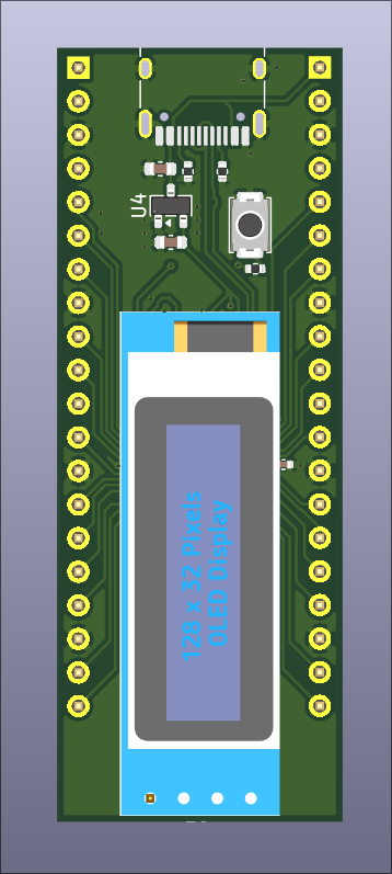
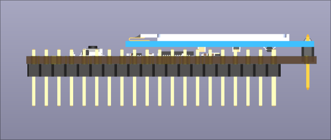
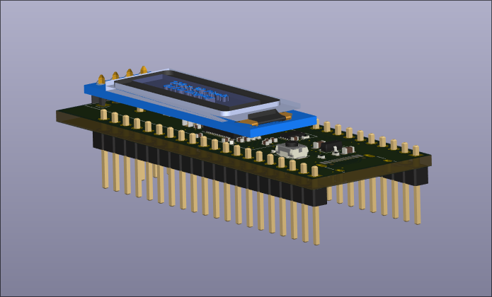
This repository documents my first PCB hardware project.
The goal was not to create a completely original product but to understand how to develop one.
I wanted to learn how devboards are designed, study each subsystem and make small modifications.
Through this project I learned:
The original inspiration came from Kai Pereira's RP2040 development board and accompanying tutorial.
✔ Schematic complete
✔ PCB routed
✔ DRC passes
Board not manufactured yet
Decided to move on to the next project - https://github.com/kyrg4z/custom-meshtastic-node
| Qty | Value | Footprint | References |
|---|---|---|---|
| 11 | 0.1uF | Capacitor_SMD:C_0402_1005Metric | C2, C3, C4, C5, C6, C7, C8, C9, C11, C12, C17 |
| 2 | 10uF | Capacitor_SMD:C_0603_1608Metric | C13, C14 |
| 2 | 1k | Resistor_SMD:R_0402_1005Metric | R5, R6 |
| 2 | 1uF | Capacitor_SMD:C_0402_1005Metric | C1, C10 |
| 2 | 27 | Resistor_SMD:R_0402_1005Metric | R3, R4 |
| 2 | 33pF | Capacitor_SMD:C_0402_1005Metric | C15, C16 |
| 2 | 5.1k | Resistor_SMD:R_0402_1005Metric | R1, R2 |
| 2 | Conn_01x20 | Connector_PinHeader_2.54mm:PinHeader_1x20_P2.54mm_Vertical | J2, J3 |
| 1 | 10k | Resistor_SMD:R_0402_1005Metric | R7 |
| 1 | 12MHz | Crystal:Crystal_SMD_3225-4Pin_3.2x2.5mm | Y1 |
| 1 | Conn_01x03 | Connector_PinHeader_2.54mm:PinHeader_1x03_P2.54mm_Vertical | J4 |
| 1 | MCP1700x-330xxTT | Package_TO_SOT_SMD:SOT-23 | U4 |
| 1 | OLED_0.49_SSD1306_I2C | Display:ER_OLEDM0.91_1x-I2C | U2 |
| 1 | RP2040 | Package_DFN_QFN:QFN-56-1EP_7x7mm_P0.4mm_EP3.2x3.2mm | U1 |
| 1 | SW_Push | Button_Switch_SMD:SW_Push_SPST_NO_Alps_SKRK | SW1 |
| 1 | USB_C_Receptacle_USB2.0_14P | Connector_USB:USB_C_Receptacle_HRO_TYPE-C-31-M-12 | J1 |
| 1 | W25Q128JVS | Package_SON:Winbond_USON-8-1EP_3x2mm_P0.5mm_EP0.2x1.6mm | U3 |

shanteacontrols/OpenDeck
A platform for building interactive control and sensing devices using MIDI and OSC built with Zephyr RTOS.


polpo/picogus
Emulation of ISA sound cards and CD-ROM on Raspberry Pi Pico (GUS, SB/Adlib, MPU-401, Tandy, CMS, Panasonic CD-ROM) with USB mouse/joystick support

Bastardkb/Dilemma
The Dilemma is a vertical stagger low-profile keyboard with mods.

Staacks/gbinterceptor
Capture or stream Game Boy gameplay footage via USB without modifying the Game Boy.


It measures 21.6 × 58.5 mm and has 2 copper layers, 1.6 mm thick.
34 parts, built around the RP2040 and W25Q128JVSIQ. The full list of its parts is on this page, with links to each part's symbol and footprint where PCBKit's library has them.
From the kyrg4z/rp2040-devboard repository on GitHub, at the commit this page was made from: the board is pcb/rp2040_devboard.kicad_pcb and its schematic pcb/rp2040_devboard.kicad_sch. PCBKit opens the board in the browser, with nothing to install.
Its repository states no licence, so its author keeps all rights: ask kyrg4z before reusing the design.