


4 layers128 × 60 mm

 kobertkirk/bldc
A KiCad hardware design plus STM32 firmware for a hall-sensored e-bike or scooter hub motor:
Bldc48 is an open-source printed circuit board by kobertkirk, from the kobertkirk/bldc repository on GitHub. It is a 4-layer board of 90 × 95 mm with 133 parts on 89 nets, routed with 1,666 tracks and 269 vias.
It is built around the STM32G431CBT6, DRV8353RSRGZ and AP2112K-3.3, with the IPT015N10N5, ESDA6V1-5SC6 and 1N4148W among its other parts. Its parts include 49 capacitors, 45 resistors, 12 connectors, 9 diodes and 8 transistors. It belongs with the STM32 boards of this library.


A KiCad hardware design plus STM32 firmware for a hall-sensored e-bike or scooter hub motor:
hardware/
  kicad/                 KiCad project (bldc48.kicad_pro): 4-sheet schematic + routed 4-layer PCB
  renders/               3D renders, routing/layer images, bldc48.glb 3D model
  bldc48-schematic.pdf   schematic as PDF
  bom.csv                bill of materials
  tools/                 circuit.py (the netlist source), generators, autorouting, connectivity checker,
                         render3d/ (VRML export + headless three.js renderer)
firmware/
  src/                   STM32G431 firmware (register-level, no HAL)
  sim/                   closed-loop PC simulation of the firmware against a hub-motor model
  cmsis/                 ST / ARM CMSIS headers (Apache-2.0)
Status — read this before building. The schematic is complete and has been checked pin by pin (see Verification). The 90 × 95 mm (3.5 × 3.7 in) 4-layer, two-sided PCB (rev F) is fully routed and passes KiCad DRC with 0 violations and 0 unconnected pads. The power stage is placed by script around fixed columns; the signal routing was done by an autorouter (Freerouting), a small grid router for what it leaves open, and scripted copper pours, so have it reviewed before ordering. The firmware compiles and passes a detailed simulation, but it has not been run on real hardware. Bring the first board up with the current-limited procedure in First power-up.
 BAT+ ──┬── TVS ── 3×1000µF + 6×2.2µF ──┬────────────────────────────────────┐
        │                                │  3 × half bridge (6 × IPT015N10N5) │
        │        ┌──────── DRV8353RS ────┴── GHx / GLx gate drive, SHx sense  ├── MOTOR A/B/C
        │        │  charge pump, 6-95 V buck → +5 V ── AP2112 → +3.3 V        │
        ├─Q1─────┤  3 × current-sense amp (G=20) ◄── 0.5 mΩ low-side Kelvin shunts
        │ latch  │  SPI config / fault readout, nFAULT
  PWR ──┘        └──► STM32G431CB ◄── ISENSE A/B/C, VBUS, throttle, NTCs
  button               │  ▲
UART ◄───┘ └── halls, FWD/REV, brake, button| Ref | Connector | Pin 1 | Pin 2 | Pin 3 | Pin 4 | Pin 5 | Pin 6 |
|---|---|---|---|---|---|---|---|
| J1 / J2 | 12 AWG solder pads (2.8 mm hole), right of the bridge | BAT+ / BAT− | |||||
| J3–J5 | 12 AWG solder pads, one per phase column | MOTOR A / B / C | |||||
| HALL | JST-GH 6 | +5 V | GND | Hall A | Hall B | Hall C | Motor NTC (optional) |
| THROTTLE | JST-GH 3 | +5 V | Signal | GND | |||
| FWD/REV | JST-GH 2 | DIR (to GND = reverse) | GND | ||||
| BRAKE | JST-GH 2 | BRAKE (to GND = braking) | GND | ||||
| POWER_BTN | JST-GH 2 | PWR_SW (momentary to GND) | GND | ||||
| UART | JST-GH 4 | +3.3 V out | TX (board → host) | RX (host → board) | GND | ||
| SWD | JST-GH 5 | +3.3 V | SWDIO | SWCLK | NRST | GND |
All signal connectors are JST-GH (1.25 mm, latching) along the bottom edge. The power button and all signal wires carry 3.3–5 V only, never battery voltage, so a cheap handlebar button is fine. Battery and phase wires are 12 AWG silicone wire soldered straight into the plated pads (strip 4 mm, push through, solder from the top; the pads are via-stitched to the pours on all layers). Strain-relieve the wires to the case or heat plate with a cable tie so the joints never carry the cable's weight. Put an XT90-S anti-spark connector and a 40 A fuse in the battery lead: the board has no reverse-polarity or inrush protection.
cd firmware && make flash).$TLM,...) appear. Type status. You should see vbus ≈ 48 V and faults NOT_DETECTED. Type drv:
it should report nFAULT=high and zero status words (the DRV8353RS took its SPI settings).detect. The wheel turns slowly forwards and then backwards (about 15 s total). Expected result:
detect OK: R = … mOhm, L = … uH, halls learned. Type save.
(No UART cable? Hold the brake and full throttle for 3 s right after power-up, then release the throttle. Detect
runs and saves automatically.)set dir_invert 1 then save.set i_batt_max 35, set i_phase_max 60,
then save.Lines end with CR or LF. Replies start with >. Telemetry lines start with $TLM (default every 100 ms;
change with stream <ms> or stream off).
$TLM,ms,state,faults,limits,vbus,ibus,power,ia,ib,ic,id,iq,iq_ref,erpm,rpm,mod,thr_v,thr_pct,dir,brake,hall,t_fet,t_mot,wh,ah,wh_regen
$TLM,105500,IDLE,0000,00,51.99,0.00,0.0,-0.01,0.01,-0.10,0.06,-0.00,0.00,2670,116.1,0.000,0.849,0.0,FWD,0,4,25.0,nan,10.912,0.2224,0.000
(Real line from the simulation: a coasting wheel at 116 rpm, 52 V, throttle at rest. t_mot is nan when no motor
NTC is enabled.)
| Command | What it does |
|---|---|
help | List the commands |
status | Human-readable state, faults, voltage, current, rpm, temperatures and control-loop CPU load |
tlm / hdr | Print one telemetry line / print the column names |
stream <ms> / stream off | Set the periodic telemetry rate, or turn it off |
get [name] | Show one parameter, or all of them (including the learned hall angles) |
set <name> <value> | Change a parameter in RAM |
save / defaults | Write the config to flash / reload the defaults into RAM |
detect / detect r / detect l / detect hall | Run auto-detect: everything, or only R, L or the hall table |
clear | Clear latched faults |
drv | DRV8353RS fault/status words, live and as captured at the last driver trip |
off / reboot | Power the board off / restart the MCU |
Main parameters (get lists them all): i_phase_max 60 A, i_batt_max 35 A, i_batt_regen 5 A, i_brake 0 A (regen
on the brake input, off by default), v_uv_start 42 V / v_uv_cut 39 V (13S), v_ov 60 V, t_fet_start 80 °C /
t_fet_max 100 °C, thr_min_v 1.0 V / thr_max_v 4.0 V, ramp_up 100 A/s, erpm_max 0 (no speed limit),
pole_pairs 23 (only affects the rpm display), mot_ntc_en 0, auto_off_min 0.
Fault bit (faults field, hex) | Meaning | Red LED blinks |
|---|---|---|
| 0x001 | overcurrent (80 A instantaneous phase-current trip) | 1 |
| 0x002 | overvoltage (> v_ov) | 2 |
| 0x004 | battery below v_uv_cut (no torque; information only) | short blink every 2 s |
| 0x008 | hall sensors invalid (000/111, e.g. unplugged) | 4 |
| 0x010 | throttle wire fault (< 0.4 V or > 4.7 V) | 5 |
| 0x020 | FET over-temperature or NTC broken | 6 |
| 0x040 | motor over-temperature (if mot_ntc_en) | 7 |
| 0x080 | halls not learned yet (run detect) | 8 |
| 0x100 | last detect failed | 9 |
| 0x200 | current-sensor offset out of range | 10 |
| 0x400 | throttle held at power-up | 11 |
| 0x800 | gate driver fault (DRV8353 nFAULT: VDS overcurrent, gate fault, UVLO, over-temperature); drv shows the fault words; the driver is re-initialised before it clears | 12 |
limits bits (why torque is reduced right now): 0x01 battery current, 0x02 phase current, 0x04 undervoltage
fold-back, 0x08 FET temperature, 0x10 motor temperature, 0x20 speed limit, 0x40 out of voltage (top speed),
0x80 stall protection.
Faults switch the gates off at once. They clear by themselves once the cause is gone and the throttle is back at zero, so the motor can never restart while the throttle is held.
Power stage. Six Infineon IPT015N10N5 (100 V, 1.5 mΩ, TOLL package) are driven directly by a TI DRV8353RS smart gate driver (100 V, SPI). It sets the gate current itself (300 mA source / 600 mA sink, ≈100 ns edges on these FETs), so there are no gate resistors; it adds 100 ns of its own dead time on top of the MCU's 400 ns and has a VDS short-circuit trip (0.3 V, ≈110 A at 125 °C) behind the firmware's 80 A trip. Its SHx inputs sense each switch node at the high-side source, right next to the gate pin. The MCU's TIM1 generates 20 kHz centre-aligned complementary PWM (6-input mode). With the main output disabled, or with the driver asleep, all six gates are held low.
Current sensing. A 0.5 mΩ 4-terminal (Kelvin) shunt sits in each low-side source (Bourns CSS4J-4026R-L500F, 5 W). Its sense pads go to one of the DRV8353RS's three current-sense amplifiers (gain 20, biased to mid-rail), so full scale is ±165 A per phase, comfortably above the 80 A hard trip (a compile-time check enforces this). The ADCs sample while all three low-side FETs conduct, triggered by TIM1 channel 4 just before the counter peak. Above 90 % duty one phase's low-side window is too short, so that phase's current is rebuilt from the other two (Ia + Ib + Ic = 0); the duty is capped at 97 % so the bootstrap capacitors always recharge.
Control. The ADCs are triggered by the PWM timer once per period, and the injected-conversion interrupt runs the FOC loop at 20 kHz:
The rotor angle comes from the halls. Each hall edge gives the exact boundary angle, and between edges the angle is extrapolated using a speed averaged over a full electrical revolution, which cancels sensor placement error. At standstill the sector centre is used, which guarantees at least 86 % torque from the very first moment.
Limits.
I_bat = 1.5·vq·iq / Vbus. In simulation it holds 34.8 A against a 35 A setting.The motor flux linkage is learned while riding and used to re-engage smoothly at speed.
Power latch. When the button is pressed it pulls Q1's base (MMBTA92, 300 V PNP) low through 47 k and a diode. Q1 enables the DRV8353RS's buck regulator. The MCU then sets PWR_HOLD, which turns on Q2 (MMBTA42) to keep Q1 on. A BAT46W blocks the button-sense pull-up, so the latch cannot creep on through the unpowered 3.3 V rail. The buck's enable divider also gives a ≈20 V UVLO. On shutdown the MCU first puts the gate driver to sleep, then releases the latch.
Supplies. The DRV8353RS's built-in 6–95 V buck (LM5008A core) makes +5 V for the halls, throttle and the
AP2112K-3.3 LDO; its 100 µH inductor is a 6 × 6 mm Bourns SRN6045TA. The gate drive comes from the DRV8353's own
charge pump (high side) and VGLS regulator (low side), so there is no 12 V rail and no separate gate-driver supply.
On power-up the firmware writes the driver's five configuration registers over SPI, reads them back and locks them;
a driver that does not answer stops the motor from starting (drv shows why).
hardware/tools/check_netlist.py exports KiCad's own netlist and checks that every pin of all 133 parts sits on
the intended net, with no single-node nets. KiCad 7's CLI has no ERC, so this replaces it. A deliberately miswired
pin is caught.
KiCad DRC on the routed PCB: 0 violations, 0 unconnected pads, 0 footprint errors, including the check that
every footprint matches the stock KiCad library (report: hardware/kicad/routing/drc.rpt).
cd firmware && make sim runs the real motor.c/hall.c/cli.c in closed loop against a model with:
dead-time, PWM delay, ADC noise and offsets, 120° halls at an arbitrary offset, a 100 kg rider and a battery with
internal resistance. It does this for two different motors. Results for motor 1:
| Check | Result |
|---|---|
| Detect R / L / hall angles | 119.9 mΩ (120) / 259 µH (250) / 0.2° worst error |
| Start from standstill, full throttle | torque ≥ 86 % of command from the first instant |
| Peak phase current | 60.2 A (limit 60 A) |
| Peak battery current (100 ms avg) | 34.3 A (limit 35 A) |
| 120 A phase-short spike | hard trip, gates off within 200 µs |
| Gate-driver fault (nFAULT) while riding | gates off within 2 PWM periods, driver re-initialised before restart |
| High-duty current rebuild (low-side shunts) | exercised continuously at top speed, no faults |
| Current-loop tracking | 0.47 A rms |
| Top speed, 26″ wheel | ≈ 39 km/h (voltage limited) |
| Coast, re-engage at speed, reverse, brake, throttle-wire break, hall unplug, low battery, overvoltage | all pass |
sudo apt install gcc-arm-none-eabi libnewlib-arm-none-eabi   # plus stlink-tools or openocd
cd firmware
make            # build/bldc48.elf/.bin/.hex  (~38 KB flash)
make flash      # st-flash, or: make flash-ocd
make sim # closed-loop simulation on the PCThe schematic, PCB and BOM are generated from hardware/tools/circuit.py, using symbols and footprints from the stock
KiCad libraries. After you edit the circuit, run hardware/tools/regen.sh. It needs KiCad ≥ 7; KiCad 8 and 9 open the
files directly.
regen.sh only places the parts. The board was then routed with
hardware/tools/route_pcb.py --legacy --no-optimize --passes 30 --freerouting freerouting-1.9.0.jar. This script:
xvfb-run)astar_route.py is a small 4-layer grid router for connections Freerouting leaves open, keeping clear of the
power copperThe routing session is saved in hardware/kicad/routing/bldc48.ses (with the DRC report next to it); route_pcb.py --ses ../kicad/routing/bldc48.ses rebuilds a routed board from it, taking the part positions from the session. The
committed bldc48.kicad_pcb is the reference: a rebuild can differ in a few fan-out vias and then needs a DRC pass.
hardware/tools/render3d/render.sh exports the board to VRML with the KiCad 3D models (plus simple stand-ins for the
JST-GH connectors, the SRN6045 inductor and the DRV8353 QFN, whose models are not in the KiCad 7 library) and renders
the PNGs in hardware/renders/ with three.js in headless Chromium; layers.sh makes the copper-layer images.
Note: regenerating overwrites placement and routing. For changes after this point, edit the board in KiCad and use Tools → Update PCB from Schematic. The footprints are already linked to their schematic symbols for that.
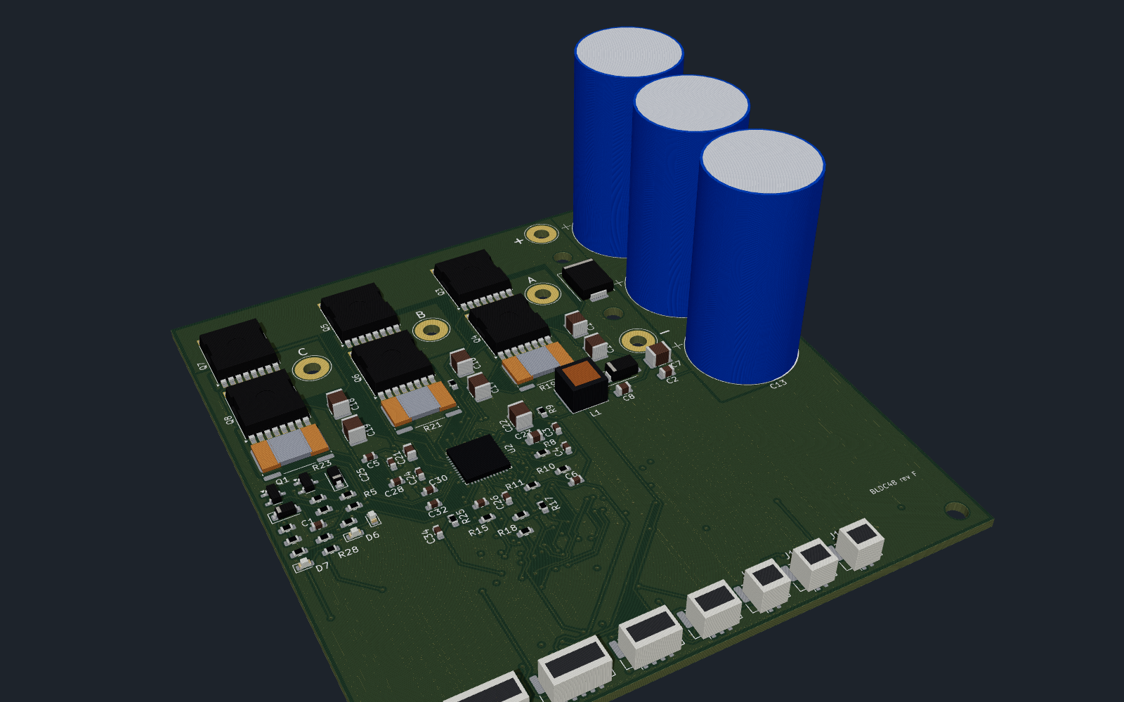
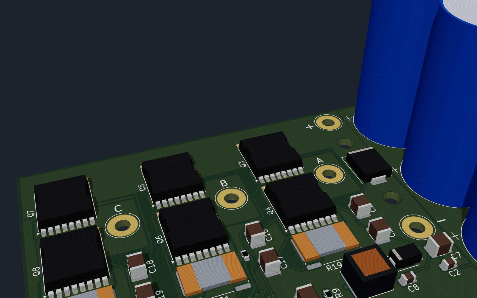
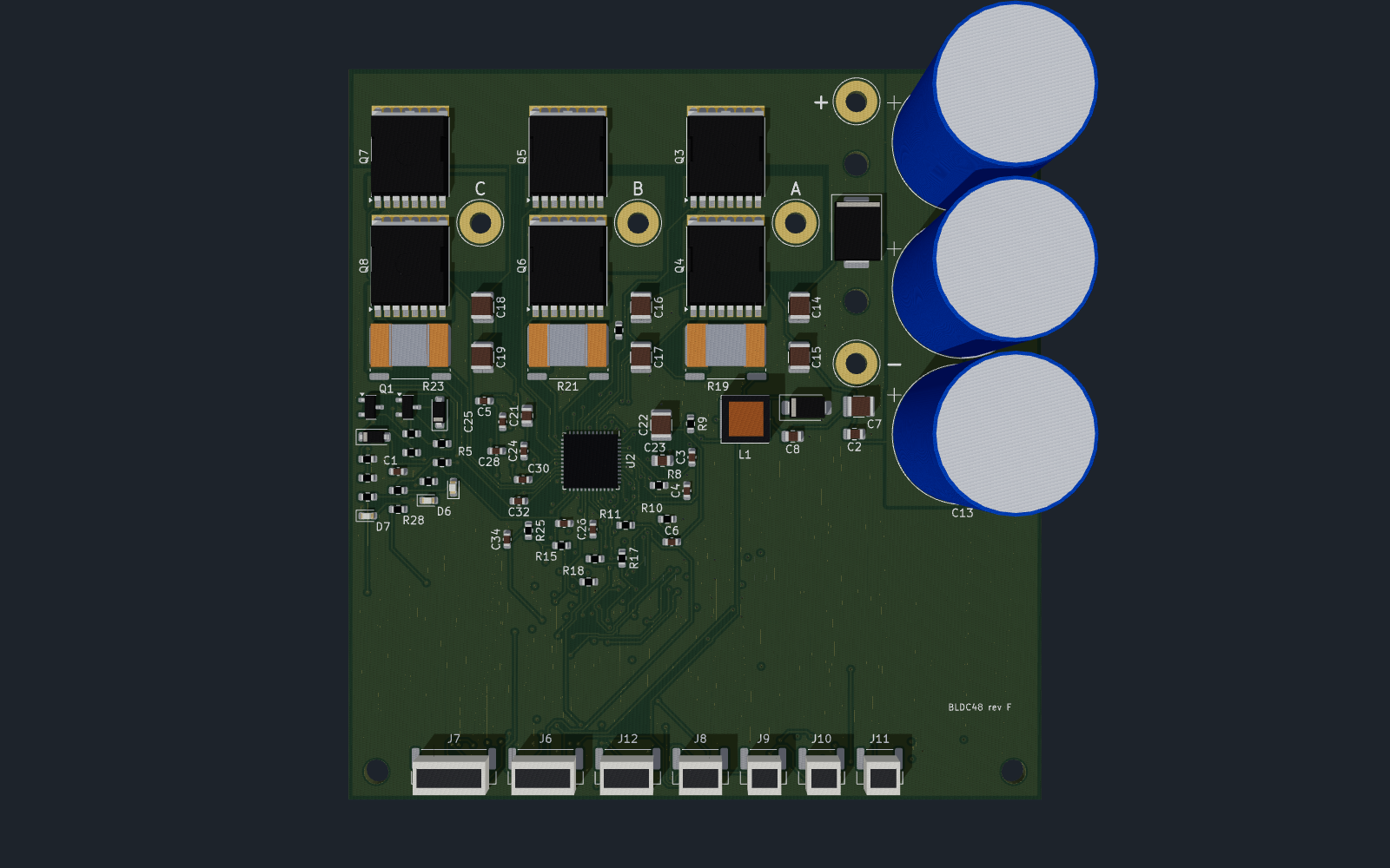
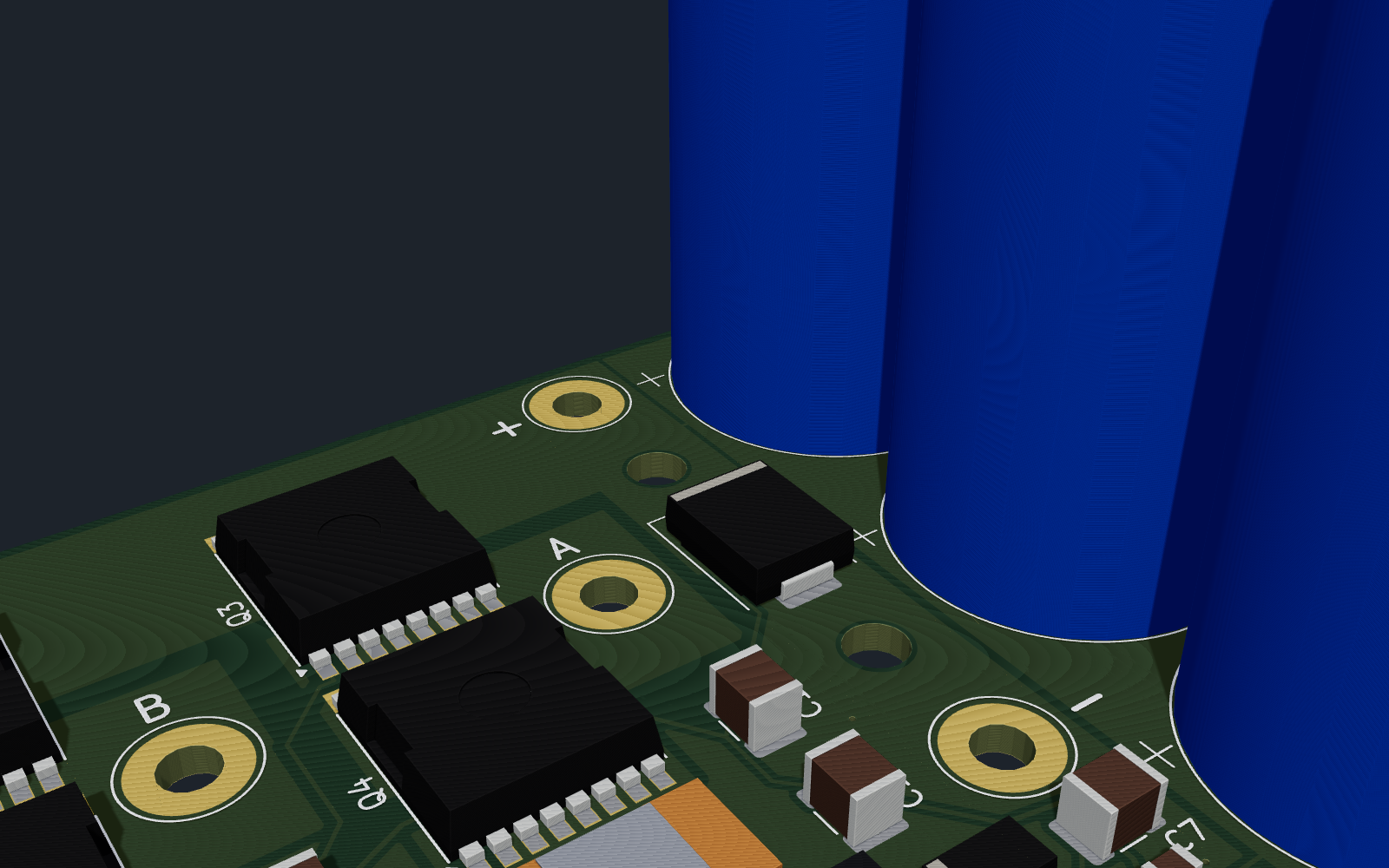
| Overview | Power stage |
|---|---|
|  |
 |  |
Routing (tracks only, pours hidden): 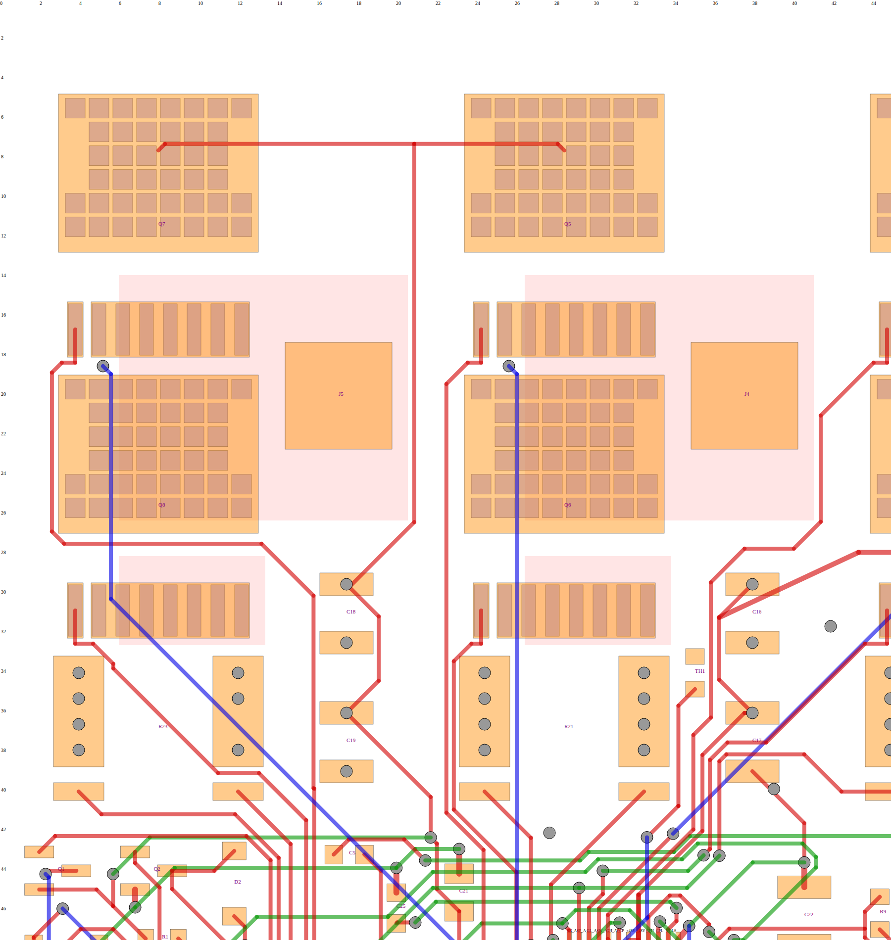
Copper layers: top · inner 1, GND · inner 2, +48V/+3V3 · bottom
Stackup as built: F.Cu power stage, gate drive and signals, with pours (switch nodes, low-side sources, +48V bus, GND fill) · In1.Cu solid GND plane · In2.Cu +48V under the power stage and +3V3 fill elsewhere, plus signals · B.Cu the same high-current pours under the bridge, the MCU and I/O parts, and signals. The inner planes are unbroken under the FETs, DC-link caps and shunts. 1666 track segments and 269 vias; each switch-node and low-side pour is one unbroken piece on both outer layers (checked by script).
Rev E (180 × 69.5 mm) was still too big. Rev F redesigns the circuit around one TI DRV8353RS smart gate driver and puts the parts on both sides of a 90 × 95 mm board, 68 % of rev E's area (3.5 × 3.7 in instead of 7.1 × 2.7 in).
Each phase is a column: high-side FET, low-side FET, shunt, two 2.2 µF ceramics and the motor wire pad on the switch node beside the FETs. The heat plate goes under the bridge (bottom side, no parts there).
These are estimates from JLCPCB's published pricing and LCSC part prices in October 2026. Upload the files to get a real quote, because their prices change often.
| Item (order of 5 assembled boards) | Approx. |
|---|---|
| 4-layer PCB 90 × 95 mm, 1.6 mm, 2 oz outer copper, 5 pcs | $30–50 |
| PCBA setup + stencils, two-sided (standard PCBA: both sides placed) | ≈ $50 |
| "Extended" LCSC part loading fee, ≈ $3 per unique part type (~22 types) | ≈ $65 |
| SMT + through-hole joints (≈ 530 SMT + 6 THT per board) | ≈ $10 |
| Parts (≈ $30/board, all from LCSC; the DRV8353RS is ≈ $6, the six FETs ≈ $15) | ≈ $150 |
| Shipping (DHL / FedEx) | $20–35 |
| Total for 5 | ≈ $325–360, about $65–72 per board |
The five 12 AWG wire pads are left for you to solder (wires are not assembled). Choosing JLCPCB's "economic" PCBA is not possible for a board with parts on both sides; if cost matters more than size, rev E (one-sided, 180 × 69.5 mm) is in the git history.
Every part in the BOM has an LCSC part number or is a generic resistor/capacitor/diode/connector that LCSC stocks in quantity, so JLCPCB can build the whole board.
i_batt_max / i_phase_max, or fit higher-ripple parts (Panasonic EEU-FC2A102, Nichicon UHE2A102).R_Shunt_Isabellenhuette_BVR4026 (same 10.6 mm span and pad layout).A full review of rev A found and fixed these problems:
| Problem in rev A | Fix in rev B |
|---|---|
| BAT+ / BAT− were 5×10 mm SMD solder pads 7.5 mm apart (≈2.5 mm copper gap), 6 mm in from the edge; SMD pads tear off under 12 AWG wire strain | M5 plated bolt terminals for ring lugs, via-stitched to the planes, on the left edge 36 mm apart, TVS between them, large BAT+/BAT− silkscreen |
| Motor pads sat 38 mm below their shunts | M5 bolt terminals on the bottom edge straight below each shunt, labelled MOTOR A/B/C |
| Overcurrent trip could never fire: INA240A2 (gain 50) saturated the ADC at ±66 A, below the 80 A trip | INA240A1 (gain 20, ±165 A full scale); a compile-time assert keeps the trip inside the measurable range; new simulation test trips on a 120 A spike within 200 µs |
| INA240 inputs tapped the switch-node/phase copper anywhere, so pour resistance corrupted the current reading | 4-terminal Kelvin shunt (Bourns CSS4J-4026R-L500F, 5 W) with dedicated sense pads to the amplifier |
| FET temperature sensor TH1 was in the board corner, far from the FETs | TH1 next to the middle low-side FET |
| DC-link ceramics ~32 mm from the low-side sources (large switching loop) | Ceramics directly under each low-side FET's source leads; both FETs drain-tab up so the switch node is a short gap between them |
| Low-side gate on the far side of the FET from its driver | Driver beside the FET pair, both gate pins facing it |
| Router ran signals on In2 straight under the FETs, slotting the +48V plane between the drains and the ceramics | Rule area keeps tracks off both inner layers under the FETs, ceramics and shunts |
| 10 Ω gate resistors: ≈170 ns edges, ≈2.9 W switching loss per high-side FET at 35 A | 4.7 Ω: ≈100 ns edges, ≈1.7 W |
| 6 × 220 µF carried ≈2.8 A rms ripple each | 8 × 220 µF, ≈2.1 A each |
| Pours sized from pad centres missed the TOLL drain tabs' real outline (vias in the tabs connected on one layer only) | Pours drawn from the measured pad outlines; inner planes solid-connected to the power terminals |
Checks run on rev B: every symbol pin matches its footprint pad (29 symbol/footprint pairs), every pin of all 174 parts is on its intended net, every footprint matches the stock KiCad library, KiCad DRC 0 violations, firmware simulation passes on two motors including the new overcurrent test.
v_uv_* for your pack. The defaults are for 13S.| Qty | Value | Footprint | References |
|---|---|---|---|
| 12 | 100n | Capacitor_SMD:C_0603_1608Metric | C27, C34, C35, C36, C37, C38, C41, C42, C46, C47, C48, C49 |
| 10 | 10k | Resistor_SMD:R_0603_1608Metric | R3, R5, R15, R17, R25, R26, R35, R39, R41, R45 |
| 9 | 1n | Capacitor_SMD:C_0603_1608Metric | C28, C29, C30, C31, C32, C33, C43, C44, C45 |
| 8 | 1k | Resistor_SMD:R_0603_1608Metric | R27, R28, R30, R32, R34, R36, R40, R42 |
| 7 | 2.2u/100V | Capacitor_SMD:C_1210_3225Metric | C14, C15, C16, C17, C18, C19, C22 |
| 6 | 100k | Resistor_SMD:R_0603_1608Metric | R1, R4, R6, R8, R13, R18 |
| 6 | IPT015N10N5 | Package_TO_SOT_SMD:Infineon_PG-HSOF-8-1 | Q3, Q4, Q5, Q6, Q7, Q8 |
| 5 | 100R | Resistor_SMD:R_0603_1608Metric | R20, R22, R24, R43, R44 |
| 4 | 1u | Capacitor_SMD:C_0603_1608Metric | C4, C9, C26, C40 |
| 4 | 2.2k | Resistor_SMD:R_0603_1608Metric | R12, R29, R31, R33 |
| 4 | M3 | MountingHole:MountingHole_3.2mm_M3 | H1, H2, H3, H4 |
| 3 | 0.5m | Resistor_SMD:R_Shunt_Isabellenhuette_BVR4026 | R19, R21, R23 |
| 3 | 1000u/100V | Capacitor_THT:CP_Radial_D18.0mm_P7.50mm | C11, C12, C13 |
| 3 | 10n | Capacitor_SMD:C_0603_1608Metric | C1, C3, C20 |
| 3 | 4.7u | Capacitor_SMD:C_0805_2012Metric | C8, C10, C39 |
| 2 | 1u/16V | Capacitor_SMD:C_0603_1608Metric | C24, C25 |
| 2 | 4.02k | Resistor_SMD:R_0603_1608Metric | R9, R10 |
| 2 | ESDA6V1-5SC6 | Package_TO_SOT_SMD:SOT-23-6 | D8, D9 |
| 2 | GREEN | LED_SMD:LED_0603_1608Metric | D5, D6 |
| 1 | 100n/100V | Capacitor_SMD:C_0805_2012Metric | C21 |
| 1 | 100u | Inductor_SMD:L_Bourns_SRN6045TA | L1 |
| 1 | 10k B3435 | Resistor_SMD:R_0603_1608Metric | TH1 |
| 1 | 12k | Resistor_SMD:R_0603_1608Metric | R37 |
| 1 | 150k | Resistor_SMD:R_0603_1608Metric | R7 |
| 1 | 1N4148W | Diode_SMD:D_SOD-123 | D2 |
| 1 | 1u/100V | Capacitor_SMD:C_0805_2012Metric | C2 |
| 1 | 22k | Resistor_SMD:R_0603_1608Metric | R38 |
| 1 | 22u/10V | Capacitor_SMD:C_1210_3225Metric | C7 |
| 1 | 330p | Capacitor_SMD:C_0603_1608Metric | C6 |
| 1 | 4.7k | Resistor_SMD:R_0603_1608Metric | R16 |
| 1 | 47k | Resistor_SMD:R_0603_1608Metric | R2 |
| 1 | 47n | Capacitor_SMD:C_0603_1608Metric | C5 |
| 1 | 47n/100V | Capacitor_SMD:C_0805_2012Metric | C23 |
| 1 | 5.6k | Resistor_SMD:R_0603_1608Metric | R14 |
| 1 | 600R@100MHz | Inductor_SMD:L_0603_1608Metric | FB1 |
| 1 | 8.2k | Resistor_SMD:R_0603_1608Metric | R11 |
| 1 | AP2112K-3.3 | Package_TO_SOT_SMD:SOT-23-5 | U1 |
| 1 | BAT+ | bldc48:SolderWire_12AWG_D2.8mm_OD5.4mm | J1 |
| 1 | BAT- | bldc48:SolderWire_12AWG_D2.8mm_OD5.4mm | J2 |
| 1 | BAT46W | Diode_SMD:D_SOD-123 | D3 |
| 1 | BRAKE | Connector_JST:JST_GH_BM02B-GHS-TBT_1x02-1MP_P1.25mm_Vertical | J10 |
| 1 | DRV8353RS | bldc48:TI-RGZ-48-QFN | U2 |
| 1 | FWD/REV | Connector_JST:JST_GH_BM02B-GHS-TBT_1x02-1MP_P1.25mm_Vertical | J9 |
| 1 | HALL | Connector_JST:JST_GH_BM06B-GHS-TBT_1x06-1MP_P1.25mm_Vertical | J7 |
| 1 | MMBTA42 | Package_TO_SOT_SMD:SOT-23 | Q2 |
| 1 | MMBTA92 | Package_TO_SOT_SMD:SOT-23 | Q1 |
| 1 | MOTOR_A | bldc48:SolderWire_12AWG_D2.8mm_OD5.4mm | J3 |
| 1 | MOTOR_B | bldc48:SolderWire_12AWG_D2.8mm_OD5.4mm | J4 |
| 1 | MOTOR_C | bldc48:SolderWire_12AWG_D2.8mm_OD5.4mm | J5 |
| 1 | POWER_BTN | Connector_JST:JST_GH_BM02B-GHS-TBT_1x02-1MP_P1.25mm_Vertical | J11 |
| 1 | RED | LED_SMD:LED_0603_1608Metric | D7 |
| 1 | SMCJ60CA | Diode_SMD:D_SMC | D1 |
| 1 | SS110 | Diode_SMD:D_SMA | D4 |
| 1 | STM32G431CBT6 | Package_QFP:LQFP-48_7x7mm_P0.5mm | U3 |
| 1 | SWD | Connector_JST:JST_GH_BM05B-GHS-TBT_1x05-1MP_P1.25mm_Vertical | J6 |
| 1 | THROTTLE | Connector_JST:JST_GH_BM03B-GHS-TBT_1x03-1MP_P1.25mm_Vertical | J8 |
| 1 | UART | Connector_JST:JST_GH_BM04B-GHS-TBT_1x04-1MP_P1.25mm_Vertical | J12 |
It measures 90 × 95 mm and has 4 copper layers, 1.6 mm thick.
133 parts, built around the STM32G431CBT6, DRV8353RSRGZ, AP2112K-3.3 and IPT015N10N5. The full list of its parts is on this page, with links to each part's symbol and footprint where PCBKit's library has them.
From the kobertkirk/bldc repository on GitHub, at the commit this page was made from: the board is hardware/kicad/bldc48.kicad_pcb and its schematic hardware/kicad/bldc48.kicad_sch. PCBKit opens the board in the browser, with nothing to install.
Its repository states no licence, so its author keeps all rights: ask kobertkirk before reusing the design.


74hc595/Panaplex-Clock
Code/schematics for a clock using a Panaplex (planar gas discharge) display

nonik0/stemmett-nixie-device
The hardware is designed in KiCad and all design files are included in the hardware directory. The hardware consists of the design of the main board PCB and three different versions of the PL31 socket breakout boards.

Hardware7253/OperationUrd
A nixie tube clock inspired by the divergence meter from Steins;Gate.

schlae/SynchroDriver
Various boards for driving synchros and other 400Hz devices
