2 layers61.3 × 63.3 mm

 KazimGL/ESP32-PowerIoT-DevBoard
ESP32 battery-powered IoT dev board with Li-ion charging, protection, and sensor support — designed in KiCad
Project CV is an open-source printed circuit board by KazimGL, from the KazimGL/ESP32-PowerIoT-DevBoard repository on GitHub. It is a 2-layer board of 76.8 × 100 mm with 62 parts on 108 nets, routed with 654 tracks and 80 vias.
It is built around the CH340C, ESP32-WROOM-32E and BME280, with the AP2112K-3.3, DW01A and TP4056-42-ESOP8 among its other parts. Its parts include 18 resistors, 9 capacitors, 6 ICs, 6 connectors and 5 diodes. It belongs with the power boards and the ESP32 boards of this library.


A battery-powered ESP32 development board with onboard Li-ion charging, protection, regulation, and sensor support — designed end-to-end in KiCad.
Designed by Kazim Bhojani (KaizBuilts [blocked]) — a fresher PCB design project built to learn the complete hardware design workflow from schematic to fabrication-ready Gerbers.
This board combines four functional subsystems into a single 2-layer PCB:
| Block | Function |
|---|---|
| Power | USB-C input, ESD protection, TP4056 Li-ion charging, DW01A + FS8205A battery protection, AP2112K-3.3 regulation, battery voltage sensing |
| Processor | ESP32-WROOM-32E module with reset/boot circuitry |
| Communication | CH340C USB-UART bridge with auto-program (DTR/RTS reset) circuit, I2C breakout |
| I/O | Dual GPIO breakout headers (1×15 each), user LED, user button, BME280 environmental sensor |
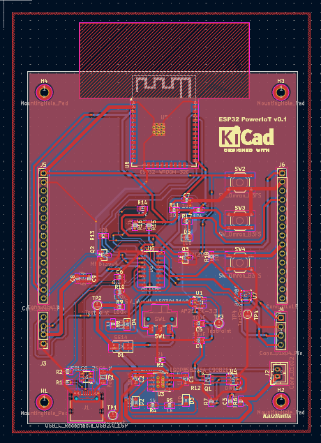
PCB Layout / Routing
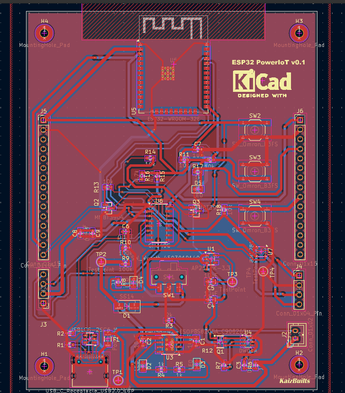
3D Render
Schematic 📄 schematic.pdf
3D Design Overview 📄 PRoject_cv.pdf
This project was built while learning PCB design fundamentals from scratch, using Claude (Anthropic) as a design-review assistant throughout the process — not to generate the design automatically, but to:
This was an intentionally iterative process: wire a section → verify in ERC → get it reviewed → fix → repeat. Every connection in this board was manually drawn, checked, and understood — the AI's role was review and explanation, not auto-generation.
Documenting these because they were the most time-consuming (and most educational) parts of the project:
KiCad global symbol library table accidentally broken — while trying to fix a missing footprint library path, the entire global symbol library table collapsed down to a single broken entry, causing 72 cascading ERC warnings across unrelated components (power, Diode, Switch, Connector libraries all failed to load). Fixed using KiCad's "Reset Libraries" button in the Symbol Libraries manager.
Custom part (FS8205A) had no native KiCad footprint — imported via easyeda2kicad from its LCSC part number, which required linking both a symbol library and a separate footprint library (.pretty folder) through two different dialogs in two different KiCad editors (Schematic Editor vs. PCB Editor) — not obvious at first.
Duplicate global labels merging unrelated nets — reused generic labels like INPUT and OUTPUT in multiple places on the schematic, which KiCad silently merged into a single net across the whole sheet, causing misleading ERC warnings until traced back and renamed to unique, meaningful net names (VBUS_FUSED, 3V3, -BATT, etc).
USB-C footprint/symbol pin-count mismatch — J1 was assigned a 6-pin "power only" USB-C footprint while the schematic symbol used the full 16-pin USB 2.0 pinout (including D+/D−), causing 10 pad-not-found errors during PCB sync. Fixed by selecting the correct 16-pin footprint (USB_C_Receptacle_HRO_TYPE-C-31-M-12) matching the real connector's datasheet.
Invalid reference designators blocking PCB sync — two LED symbols were accidentally named Green(Done)1 and RED(charging)1 instead of standard alphanumeric designators, which KiCad's schematic/ERC tolerated but the PCB sync step rejected outright. Renamed to proper D4/D5 format.
DRC hole-size violation on the ESP32 module footprint — the ESP32-WROOM-32E footprint's castellated pads required a 0.2mm minimum drill size, but the board's design rules were set to a 0.3mm minimum, causing 21 repeated violations. Resolved by adjusting the board's minimum drill size constraint to match both the footprint and the target fab's actual capability.
Incomplete thermal relief connections on copper pour zones for small shield/ground pads — fixed by reducing the thermal relief gap and spoke width settings to better fit smaller pad geometries.
Each of these was worked through methodically: understand the error → identify root cause → fix → re-verify, rather than blindly applying fixes.
project_CV.kicad_pro    → KiCad project file
project_CV.kicad_sch    → Schematic source
project_CV.kicad_pcb    → PCB layout source
schematic.pdf           → Exported schematic (all 4 blocks)
PRoject_cv.pdf          → Full project document
*.png                   → PCB layout / 3D render screenshots
README.md → This fileBuilt as a learning project to understand the full PCB design lifecycle — schematic capture, component selection, DFM, fabrication file generation, and bring-up — end to end.
| Qty | Value | Footprint | References |
|---|---|---|---|
| 5 | 10k | Resistor_SMD:R_0603_1608Metric | R11, R12, R13, R14, R18 |
| 5 | 1k | Resistor_SMD:R_0603_1608Metric | R4, R5, R7, R8, R17 |
| 4 | 0.1uF | Capacitor_SMD:C_0603_1608Metric | C3, C6, C8, C9 |
| 4 | 10uF | Capacitor_SMD:C_0805_2012Metric | C1, C2, C4, C5 |
| 4 | LED | LED_SMD:LED_0805_2012Metric | D2, D3, D4, D5 |
| 4 | MountingHole_Pad | MountingHole:MountingHole_2.2mm_M2_Pad | H1, H2, H3, H4 |
| 4 | TestPoint | TestPoint:TestPoint_Pad_D2.0mm | TP1, TP2, TP3, TP4 |
| 3 | SW_Omron_B3FS | Button_Switch_SMD:SW_SPST_TL3342 | SW2, SW3, SW4 |
| 2 | 100k | Resistor_SMD:R_0603_1608Metric | R9, R10 |
| 2 | 4.7k | Resistor_SMD:R_0603_1608Metric | R15, R16 |
| 2 | 5.1k | Resistor_SMD:R_0603_1608Metric | R1, R2 |
| 2 | Conn_01x04_Pin | Connector_PinHeader_2.54mm:PinHeader_1x04_P2.54mm_Vertical | J3, J4 |
| 2 | Conn_01x15 | Connector_PinHeader_2.54mm:PinHeader_1x15_P2.54mm_Vertical | J5, J6 |
| 2 | MMBT3904 | Package_TO_SOT_SMD:SOT-23 | Q2, Q3 |
| 1 | 100 | Resistor_SMD:R_0603_1608Metric | R6 |
| 1 | 1uF | Capacitor_SMD:C_0603_1608Metric | C7 |
| 1 | 2k | Resistor_SMD:R_0603_1608Metric | R3 |
| 1 | AP2112K-3.3 | Package_TO_SOT_SMD:SOT-23-5 | U1 |
| 1 | BME280 | Package_LGA:Bosch_LGA-8_2.5x2.5mm_P0.65mm_ClockwisePinNumbering | U7 |
| 1 | CH340C | Package_SO:SOIC-16_3.9x9.9mm_P1.27mm | U6 |
| 1 | Conn_01x02 | Connector_JST:JST_PH_B2B-PH-K_1x02_P2.00mm_Vertical | J2 |
| 1 | DW01A | Package_TO_SOT_SMD:SOT-23-6 | U4 |
| 1 | ESP32-WROOM-32E | RF_Module:ESP32-WROOM-32E | U5 |
| 1 | FS8205A_C908265 | FS8205A_lib:SOT-23-6_L2.9-W1.6-P0.95-LS2.8-BR | Q1 |
| 1 | Polyfuse | Fuse:Fuse_1206_3216Metric | F1 |
| 1 | SS14 | Diode_SMD:D_SMA | D1 |
| 1 | SW_Wuerth_450301014042 | Button_Switch_SMD:SW_SPDT_CK_JS102011SAQN | SW1 |
| 1 | TP4056-42-ESOP8 | Package_SO:SOIC-8-1EP_3.9x4.9mm_P1.27mm_EP2.41x3.3mm_ThermalVias | U3 |
| 1 | USBLC6-2SC6 | Package_TO_SOT_SMD:SOT-23-6 | Ue |
| 1 | USB_C_Receptacle_USB2.0_16P | Connector_USB:USB_C_Receptacle_HRO_TYPE-C-31-M-12 | J1 |
The 61 most common of 62 parts.
It measures 76.8 × 100 mm and has 2 copper layers, 1.6 mm thick.
62 parts, built around the CH340C, ESP32-WROOM-32E, BME280 and AP2112K-3.3. The full list of its parts is on this page, with links to each part's symbol and footprint where PCBKit's library has them.
From the KazimGL/ESP32-PowerIoT-DevBoard repository on GitHub, at the commit this page was made from: the board is project_CV.kicad_pcb and its schematic project_CV.kicad_sch. PCBKit opens the board in the browser, with nothing to install.
Its repository states no licence, so its author keeps all rights: ask KazimGL before reusing the design.

Salma-lotfy-Wazery/esp32-battery-powered-iot-node
Custom 2-layer PCB designed in KiCad featuring ESP32, integrated LiPo charging (TP4056), USB-C power delivery, and sensor telemetry.

houseofthe051010/ESP32-Walkie-Talkie-V2
This ESP32 Walkie Talkie is redesigned with a SX1262 radio, a PCB, and a full case redesign.

ZharbolatDinmukhamed/Haptic-Glove-PCB
A wrist-mounted PCB for a haptic feedback glove, developed as part of my Research Assistantship at the Tactile Laboratory, Nazarbayev University.

jonny190/TableLight
A 3D-printable, battery-powered, USB-C rechargeable table lamp in the classic "Poldina" shape - honeycomb disc base, thin stem, down-firing cone shade with a white top - running WLED on an ESP32, with a capacitive touch…

HYLDAIC/Flagshep-V1_Audio-Player
A high fidelity semi-portable audio player student project with provided PCB files, 3D files and Code

Matyas604/Pocket-lightning-detector
A lightning detector that runs on a battery and fits in your pocket. It records the distance, energy and current time of a lightning strike, and you can then view this data via Bluetooth in mobile app.
