4 layers95 × 60 mm

 karimf1/J939-transceiver
This project is an isolated CAN/J1939 transceiver breakout on a 2-layer board. It includes a DE-9 or terminal block and termination jumper. It demonstrates a complete PCB design workflow: custom symbol/footprint creation, layout, DRC, ordering, hand-soldering, and testing.
Can iso is an open-source printed circuit board by karimf1, from the karimf1/J939-transceiver repository on GitHub, published under the MIT licence. It is a 2-layer board of 100 × 50 mm with 41 parts on 28 nets, routed with 126 tracks and 48 vias.
It is built around the ISO1042BDWVR, NXE1S0505MC-R7 and BAT54, with the SMAJ36CA and DMG2301L among its other parts. Its parts include 9 capacitors, 7 resistors, 7 diodes, 3 connectors and 2 ICs. It belongs with the radio and wireless boards of this library.


A galvanically isolated CAN transceiver on a 100 × 50 mm two-layer board: DE-9 wired to CiA 303-1, a 5-way terminal block carrying the same nets in parallel, split 120 Ω termination on a jumper, and bus-side power generated across the barrier.
The circuit is deliberately trivial — one transceiver, one isolated supply, a connector and two resistors. That is the point. A trivial circuit is the only kind that lets you walk the whole hardware pipeline without the circuit itself becoming the project: a symbol and a footprint drawn by hand from a datasheet, a schematic, a netlist, a board, a fabrication package.
What makes it worth reading is what the datasheets said on the way through, and one number that is measured rather than asserted.
Status: designed, not built. No board has been ordered, so there are no bench results here — every number below is derived from a datasheet or read out of the board file.
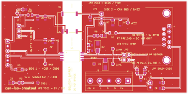
An isolation barrier is a claim, and claims should have numbers. Sorting every piece of copper onto one side of the board by net and measuring the gap gives:
| mm | what it means | |
|---|---|---|
| layout clearance, side 1 ↔ side 2 | 10.300 | the closest approach the layout is responsible for |
| U1 land pattern (TI DWV0008A) | 9.100 | the transceiver's own recommended footprint |
| U2 land pattern (Murata NXE1) | 4.080 | the isolated supply module's |
| shortest path via floating copper | 6.621 | two hops, via U2's mechanical pad 14 |
| assembly clearance | 4.080 | what the finished board actually is |
The isolation rating of an assembly is the minimum over its components, and
here that minimum is not the isolator. U1 is 5000 VRMS for one
minute with 8.5 mm of creepage; U2 is 3000 VDC with 4.08 mm between
its pad rows. Fitting both and calling the board a 5 kV part would be wrong by
nearly a factor of two. So it is a 3 kV assembly, and the silkscreen says
U1 5kVrms / U2 3kVdc with both ratings side by side.
There is a configuration on the board that gets the transceiver's full rating: leave U2 unpopulated and take bus-side power from DE-9 pin 9 through JP2. Then nothing crosses the barrier but U1, and the clearance becomes 9.1 mm. That is what the JP2 jumper is for.
Full working in docs/isolation.md.
The Murata NXE1 is an unregulated, open-loop converter. Buried in its notes:
The minimum load to meet datasheet specification is 10% of the full rated load … Lower than 10% minimum loading will result in an increase in output voltage, which may rise to typically double the specified output voltage if the output load falls to less than 5%.
The ISO1042 draws 2.8 mA on the bus side when the bus is recessive. That is 1.4 % of the module's 200 mA rating — below the 5 % cliff. An unloaded barrier supply would push roughly 10 V into a part whose absolute maximum VCC2 is 6 V. Every board, every time, before a single frame was sent.
The fix is R7, a 240 Ω preload, holding the module at 12.8 % of rating no
matter what the bus is doing. It costs 104 mW and it is the difference between
a board that works and a board that kills a $5 transceiver on the bench. D7, a
5.6 V zener, is the backstop for the day someone builds one and leaves R7 off.
The silkscreen says R7 PRELOAD - DO NOT OMIT.
The standard bus-protection diode for CAN is a 24 V stand-off part, chosen for transceivers with a ±12 V common-mode range. The ISO1042's common-mode range is ±30 V. A 24 V TVS would conduct inside the transceiver's own legal operating range — it would clamp the bus during exactly the ground offset this board exists to survive.
So D2 and D6 are 36 V stand-off, bidirectional, clamping below the ±70 V bus fault rating: a window bounded below by the transceiver's common-mode range and above by its fault rating.
A CAN bus is a differential bus with a limited common-mode range. Two nodes on different chassis, different supplies, or 30 m of cable apart do not share a ground — they share a ground offset. A non-isolated transceiver survives that offset up to its common-mode limit and then the link stops working, or the part stops existing.
The board is the isolated node. A $2 non-isolated module is the control group. Sweeping a DC offset between the two nodes' grounds and plotting frame error rate for each should give a flat line at zero for the isolated board and a cliff for the other. That turns received wisdom into a graph, which is the difference between a project and a tutorial.
The firmware is written for it: fw/j1939_rx counts frames against a
sequence number the transmitter embeds, so the error rate comes from counting
rather than from an assumption about timing.
Everything except U1 and U2 comes from KiCad's standard libraries. Those two
are drawn from their datasheets into hw/lib/, because "draw a part
from a datasheet" is the skill this board exists to demonstrate.
TI_DWV0008A — the ISO1042's 8-pin wide-body SOIC. Every number is off
drawing 4218796/A in the datasheet: 10.9 mm land row spacing, 1.8 × 0.6 mm
pads, 1.27 mm pitch, 0.07 mm solder-mask expansion, 11.5 mm lead span. The
resulting gap between the rows is 9.1 mm, which matches the datasheet's own
9.1 mm NOMINAL CLEARANCE/CREEPAGE note exactly.
The footprint also carries a keepout zone across its own barrier, so the rule that no copper may sit between the pad rows travels with the part instead of living only in someone's memory.
NXE1S0505MC — the isolated supply, including pad 14, which Murata
documents as "not available for electrical connection" and which is therefore
deliberately left off the netlist rather than tied to ground.
The schematic and the PCB are emitted by Python rather than placed in the GUI. The reason is not speed — 25 parts do not need a generator — it is that a generator can carry a rule the human eye does not enforce: no net and no part may touch both sides of the barrier. That invariant is expressed once, in code, and it holds before the board exists. Everything else the generator buys (reproducible geometry, a canonical digest of every part position and track) is a consequence of that choice rather than the reason for it.
| parameter | value | why |
|---|---|---|
| Protocol | CAN 2.0B, 29-bit IDs, J1939-compatible PHY | J1939 is CAN 2.0B on a defined physical layer |
| Bit rate | 250 kbit/s (J1939-11/-15), 500 kbit/s (J1939-14) | loop delay allows 157 m and 57 m respectively |
| Logic side | 1.71 – 5.5 V, JP1 selects 5 V or 3V3 from the host | RXD swings to whatever the host runs at |
| Bus side | 5 V, from U2 or from DE-9 pin 9 (JP2) | the bus side must not need a second power brick |
| Isolation | 3 kVDC as built; 5 kVRMS with U2 unpopulated | set by the weakest component, stated on the silkscreen |
| Bus fault tolerance | ±70 V | 24 V truck electrics; a shorted bus line is routine |
| Common-mode range | ±30 V | which is why the TVS is a 36 V part |
| Termination | 120.8 Ω split (2 × 60R4 + 4n7), jumper-selectable | TI's own characterisation network |
| Host draw | 164 mA worst case, ~40 mA idle | fits a USB-powered dev board |
| Board | 100 × 50 mm, 2 layer, 1.6 mm | JLCPCB standard process, no special features |
PLAN.md was written first and mostly held. Four deviations, all decided for a reason:
The plan's §3.2 called the unregulated module "the single most likely 'it works but marginally' failure in this design." It was not marginal, and it was found by reading the notes section.
| Qty | Value | Footprint | References |
|---|---|---|---|
| 3 | 100n | Capacitor_SMD:C_0805_2012Metric | C2, C4, C9 |
| 3 | 4u7 | Capacitor_SMD:C_0805_2012Metric | C5, C6, C7 |
| 2 | 1k5 | Resistor_SMD:R_0805_2012Metric | R3, R6 |
| 2 | 4n7 | Capacitor_SMD:C_0805_2012Metric | C1, C8 |
| 2 | 60R4 1% | Resistor_SMD:R_0805_2012Metric | R1, R2 |
| 2 | BAT54 | Diode_SMD:D_SOD-123 | D1, D5 |
| 2 | SMAJ36CA | Diode_SMD:D_SMA | D2, D6 |
| 2 | green | LED_SMD:LED_0805_2012Metric | D3, D4 |
| 1 | 100k | Resistor_SMD:R_0805_2012Metric | R4 |
| 1 | 1M | Resistor_SMD:R_0805_2012Metric | R5 |
| 1 | 1u | Capacitor_SMD:C_0805_2012Metric | C3 |
| 1 | 240R 1% | Resistor_SMD:R_1206_3216Metric | R7 |
| 1 | 5V6 | Diode_SMD:D_SOD-123 | D7 |
| 1 | 600R@100MHz | Inductor_SMD:L_0805_2012Metric | FB1 |
| 1 | CANH | TestPoint:TestPoint_Pad_D1.5mm | TP1 |
| 1 | CANL | TestPoint:TestPoint_Pad_D1.5mm | TP2 |
| 1 | DE-9 male, CiA 303-1 | Connector_Dsub:DSUB-9_Pins_Horizontal_P2.77x2.84mm_EdgePinOffset9.90mm_Housed_MountingHolesOffset11.32mm | J2 |
| 1 | DMG2301L | Package_TO_SOT_SMD:SOT-23 | Q1 |
| 1 | GND1 | TestPoint:TestPoint_Pad_D1.5mm | TP7 |
| 1 | GND2 | TestPoint:TestPoint_Pad_D1.5mm | TP3 |
| 1 | Host 1x06 | Connector_PinHeader_2.54mm:PinHeader_1x06_P2.54mm_Vertical | J1 |
| 1 | ISO1042BDWVR | can-iso:TI_DWV0008A | U1 |
| 1 | MKDS 1,5/5-5.08 | TerminalBlock_Phoenix:TerminalBlock_Phoenix_MKDS-1,5-5_1x05_P5.00mm_Horizontal | J3 |
| 1 | NXE1S0505MC | Converter_DCDC:Converter_DCDC_Murata_NXExSxxxxMC_SMD | U2 |
| 1 | RXD | TestPoint:TestPoint_Pad_D1.5mm | TP6 |
| 1 | SHLD hard bond | Connector_PinHeader_2.54mm:PinHeader_1x02_P2.54mm_Vertical | JP4 |
| 1 | TERM 120R | Connector_PinHeader_2.54mm:PinHeader_2x02_P2.54mm_Vertical | JP3 |
| 1 | TXD | TestPoint:TestPoint_Pad_D1.5mm | TP5 |
| 1 | VCC1 = 5V / 3V3 | Connector_PinHeader_2.54mm:PinHeader_1x03_P2.54mm_Vertical | JP1 |
| 1 | VCC2 | TestPoint:TestPoint_Pad_D1.5mm | TP4 |
| 1 | VCC2 = DCDC / bus | Connector_PinHeader_2.54mm:PinHeader_1x03_P2.54mm_Vertical | JP2 |

ryanbjohnson/PentairMasterTempESP32
This folder is the KiCad project area for the MasterTemp 125 ESP32 interface board.


AndreiVladescu/LibrePLC32
The goal of the project is to create a compact, hackable, and well-documented PLC platform for industrial automation experiments, prototyping, education, and open hardware development.

Queens-Rocket-Engineering-Team/Avionics-23-26
QRET Avionics hardware, firmware, and documentation for 2023 to 2025.


Gad9889/Thermistor-Expansion-Module
KiCad project files remain at the repository root. Hierarchical schematic sheets are organized under schematics/, with connector sheets in schematics/connectors/ and gate sheets in schematics/gates/.

jgrano/Nx-PCBA
Install all of these before opening the project:
It measures 100 × 50 mm and has 2 copper layers, 1.6 mm thick.
41 parts, built around the ISO1042BDWVR, NXE1S0505MC-R7, BAT54 and SMAJ36CA. The full list of its parts is on this page, with links to each part's symbol and footprint where PCBKit's library has them.
From the karimf1/J939-transceiver repository on GitHub, at the commit this page was made from: the board is can-iso.kicad_pcb and its schematic can-iso.kicad_sch. PCBKit opens the board in the browser, with nothing to install.
Its repository publishes it under the MIT licence: you may reuse it on that licence's terms (keep the author's notice, and for a copyleft licence share your changes alike).