4 layers100 × 77 mm

 karimf1/rover-panel-pcb
This repository is continuation of rover panel repo. Power panel PCB layout is implemented in KiCAD based of AutoCAD version of rover panel .
Rover panel supervisor is an open-source printed circuit board by karimf1, from the karimf1/rover-panel-pcb repository on GitHub, published under the MIT licence. It is a 2-layer board of 110 × 46 mm with 106 parts on 54 nets, routed with 802 tracks and 205 vias.
It is built around the LM5165XDRC, 74LVC1G08Z and LM339, with the SN74LVC1G74DCU, 2N7002K and PESD5V0S1BA among its other parts. Its parts include 38 resistors, 18 capacitors, 18 diodes, 12 transistors and 5 ICs. It belongs with the robots and motor control boards of this library.


The PCB was missing. It sits on four standoffs on the panel plate, between the shunt and the signal connector, and does three jobs:
R1
into the ESC bank, and holds contactor K1 open until the switched bus
reaches ~90 % of the packK1's coil is energised through the E-stop loop and this
board, so the board can open K1 but nothing on it can close K1 past an
open E-stopRS1, reported
over I2C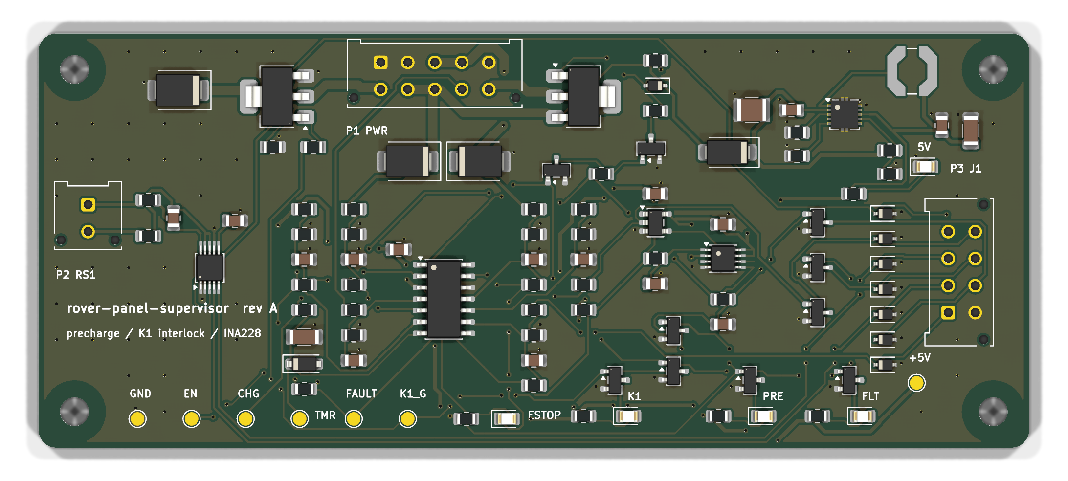
It replaces two of the panel's bought parts — K2, an automotive precharge
relay, and A1, an INA228 breakout on standoffs — and it answers two of the
panel's open questions: "precharge is sized by hand and is not in any check"
and "is the E-stop hard-wired in series with the contactor coil?"
The one claim the board is built to prove:
K1 cannot close unless the E-stop loop is closed AND the host has raised a fresh ARM edge AND the switched bus has reached the precharge threshold — and that is hardware, checked against the exported netlist, not a promise made by firmware. There is no firmware.
The logic is four comparators, one AND gate and one D flip-flop. Every node that feeds the interlock is an open-collector output pulled up to EN, not to 5 V — so the instant the board disarms, every one of them falls with it.
| signal | made by | means |
|---|---|---|
ESTOP_OK | U3C: the far side of the E-stop loop (COIL_POS) above 13.7 V | the mushroom switch is closed |
ARM | U3D: host line above 1.37 V, 100 k pull-down | the host asked; an unplugged harness reads as no |
CLR# | U4: ARM AND ESTOP_OK | either one dropping clears the latch immediately |
EN | U5 (74LVC1G74) Q, set only on a rising edge of ARM delayed 10 ms | armed |
CHG | U3A: switched bus / always-on bus below the threshold | precharging |
FAULT | U3B: CHG has been high longer than the timer (≥ 1.68 s) | the bus is not charging — latches |
K1_G | EN, pulled low by CHG (Q2) or FAULT (Q3), 1 ms RC | close the contactor |
PRE_G | EN, pulled low by FAULT (Q4) | precharge switch on |
The flip-flop is there for one reason. With a plain AND gate, releasing the
E-stop while the host is still asserting ARM would re-energise the drive
motors on its own. With the latch, an E-stop release does nothing until the
host drops ARM and raises it again. That is what competition rules mean by
a deliberate restart, and it is scenario 5 in the simulation below.
The K1 coil path is:
+24 V -> P1.8 -> J1 -> E-stop -> J1 -> P1.3 -> P1.4 -> K1 coil -> P1.6 -> Q1 -> GNDQ1 is on the low side. It can only interrupt that loop.
The comparator does not measure "90 % of 24 V". It compares two dividers —
the switched bus against the always-on bus — so it holds from a 21 V cutoff
to a 29.4 V full pack. Its threshold still moves, for three reasons, and
calcs.pre_ratio_window() takes every corner of all three:
precharge threshold window     88.34 .. 91.74 % of pack
bus can reach through R1       94.50 % at 21 V, with 50 mA of ESC idle draw
The ESC idle draw is the constraint. The bus charges towards
V − I_idle × R1, not towards V. At a 21 V pack and 50 mA of idle current,
R1 takes 1.1 V off the target, and a threshold set at the textbook 95 % would
never be reached — the board would fault on every power-up. The 50 mA is
assumed and is the first thing to measure (§6).
precharge time, nominal        0.41 s    (6 mF, 25.9 V)
precharge time, worst          0.73 s    (9 mF, 21 V, highest threshold)
fault timer                    1.68 / 2.36 / 2.66 s   (min / nom / max)
The minimum assumes the 10 µF X7R timing capacitor has lost 25 % to tolerance
and DC bias, and that the comparator's full bias current is helping to charge
it. That still leaves 2.3× margin over the slowest legitimate precharge. The
maximum is bounded too: into a dead short, R1 sees 41 W, inside its 50 W
continuous rating, for as long as the timer takes.
The panel's params.py reserves a supply for the board: a 2 A time-lag fuse on
DIN2-203, 18 AWG, 0.2 A continuous and a 2.5 A peak. The panel's
sizing.py sizes the wiring from those numbers, and this board checks that
its worst case fits inside them. Neither side can quietly outgrow the other.
24 V draw                      76 mA continuous (70 mA of it is K1's hold current)
2.17 A worst instant: K1 pull-in while precharge still conducts| check | result |
|---|---|
INA228 full scale at ADCRANGE = 0 | 218 A, 0.42 mA per count, SHUNT_CAL = 2803 |
| current error at 10 A | 0.31 % (shunt 0.25 %, INA228 gain, offset, filter bias) |
| input TVS SM6T36A | stands off 30.8 V > 29.4 V; clamps 49.9 V < 60 V (every FET on the 24 V side) |
| K1 FET gate drive | 4.85 V on a 5 V −2 % rail, ≥ the 4.5 V its RDS(on) is quoted at |
| K1 coil at pack cutoff | 19.8 V ≥ 16 V pickup, after the E-stop loop, the FET and panel wiring |
| precharge FET gate | zener-clamped, ≤ 12.6 V worst case, from 21 V to 29.4 V (fully on, under ±20 V) |
| every LM339 input | inside VCC − 1.5 V at a full pack |
| power traces | 1.0 mm vs 0.70 mm IPC-2221 at 2.5 A as if continuous |
test_calcs.py finishes with a 1 ms-step simulation of the interlock built
from those same thresholds and time constants — nothing retuned for the test:
PASS  power-up, ARM low: nothing switches
PASS  ARM with a healthy bus (3 mF): precharge, then K1, no fault  -- K1 closes 0.20 s after ARM, bus at 90.7 %
PASS  ARM with a healthy bus (9 mF): precharge, then K1, no fault  -- K1 closes 0.58 s after ARM, bus at 90.7 %
PASS  ARM into a shorted bus: FAULT latches, precharge stops, K1 never closes  -- fault 2.36 s after ARM
PASS  E-stop opens while K1 is closed: K1 drops within 1 ms
PASS  E-stop released with ARM still high: K1 stays OPEN (needs a new ARM edge)
PASS  ARM cycled after the E-stop reset: precharge and K1 again
PASS  FAULT holds for as long as ARM stays high (a latch, not a retry loop)
PASS dropping ARM clears FAULT and leaves everything offARM AND E-STOP AND PRECHARGED.
Writing scenario 4 of the simulation showed what that does: release the
E-stop with ARM still high and the motors come back on by themselves.
The 74LVC1G74 and its 10 ms clock delay are the fix. KiCad 9 ships no
74LVC1G74 symbol, so it is generated from a pin map in spec.py
(hw/gen/gen_lib.py).VERIFY.)K1 above and to the DIN2 terminals below
leaves 46 mm. Width was the only direction left to grow.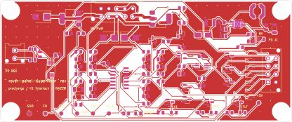
Placement is by hand, in hw/gen/gen_pcb.py, because placement is the
layout design:
K1 and R1.
Its edge row is ground plus the E-stop-return/coil+ pair, which never has
to leave the connector. Every net that travels is on the inner row.RS1. The INA228 is
turned so its inputs face P2 and its I2C and ground pins face open board.J1) is on the right edge, with the ESD diodes in a
column in the same order as its pins.The copper between the pads comes from hw/gen/autoroute.py: a 0.1 mm grid
A* router, two layers, that runs inside KiCad's own Python using numpy.
None of that is trusted. kicad-cli DRC with schematic parity is the judge.
802 track segments, 1753 mm of track (181 mm on B.Cu, the ground plane)
205 vias, all tented
0 DRC violations, 0 unconnected pads, 0 footprint errorshw/gen/check_interlock.pyThis reads the netlist KiCad exported, not the generator, and checks the structure the simulation assumes:
PASS  no on-board path from +24V_IN to COIL_POS, even with every FET on
PASS  COIL_POS touches only P1, a clamp to GND and a >= 100 k sense resistor  -- D6 TVS to ['GND'], R18 100k
PASS  the ONLY thing that can raise K1_G is one resistor from EN  -- pull-ups ['R29->EN']
PASS  K1_G is held low by precharge-in-progress (CHG) and by FAULT  -- Q2(gate CHG), Q3(gate FAULT)
PASS  EN is driven by U5.Q (pin 5) and nothing else
PASS  U5 D and /PRE are tied high: it can only SET on a clock edge
PASS  U5 /CLR = U4 output = ARM AND ESTOP_OK
PASS  VE is a divider off COIL_POS -- the FAR side of the E-stop loop
...                                                          24 checks
And a test for the test. A structural check that passes on a correct
netlist proves nothing unless it fails on a wrong one.
test_interlock_check.py applies six plausible mistakes to copies of the
netlist. It requires each one to be caught by the specific check written for
it:
PASS  a 100 ohm part bridging +24V_IN straight to the coil  -- caught by: no on-board path from +24V_IN to COIL_POS
PASS  K1_G pull-up taken from +5V instead of EN (E-stop and ARM bypassed)  -- caught by: the ONLY thing that can raise K1_G
PASS  E-stop sense divider moved to the pack side of the loop  -- caught by: VE is a divider off COIL_POS
PASS  flip-flop /CLR tied high (a released E-stop would re-arm by itself)  -- caught by: U5 /CLR = U4 output
PASS  precharge comparator reading the always-on bus twice  -- caught by: VA divides +24V_IN and VS divides SW_SENSE
PASS FAULT no longer holds K1 off (Q3 gate moved to GND) -- caught by: K1_G is held low by precharge-in-progresshw/gen/check_layout.pyA board can pass DRC with a 0.3 mm tap carrying the coil current. This script checks the saved board:
On its first run it failed three times, and only one of those was the board:
Reviewing that output also turned up a problem the check had let through: its 30 mm limit had let the coil+ clamp sit 28 mm from its pin. D6 now sits under P1, and the limit is 12 mm.
hw/gen/check_fit.pyThe plate was drilled from the panel's params.py. The board was built from
panel_interface.json, which params.py wrote. This script reads the
finished .kicad_pcb back through pcbnew and compares it against
params.py imported live, so a stale JSON, a hand-edited board and a moved
plate hole all fail:
PASS  panel_interface.json is not stale (equals params.pcb_interface() now)
PASS  H1 at (4.00, 4.00) is where params.py put it  -- params (4, 4) dia 3.2, board dia 3.20
...
PASS  every board hole lands on a plate hole (panel frame)  -- plate [(236.0, 222.0), (236.0, 260.0), (338.0, 222.0), (338.0, 260.0)]
PASS  P1 sits on the top edge, facing its panel device  -- pads centred 4.7 mm from the top edge
PASS  P2 sits on the left edge, facing its panel device  -- pads centred 5.5 mm from the left edge
PASS  P3 sits on the right edge, facing its panel device  -- pads centred 7.5 mm from the right edge
PASS standoff + board + tallest mated connector fits the height params.py allows -- 10 + 1.6 + 25 = 36.6 mm <= 36.6 mm| Qty | Value | Footprint | References |
|---|---|---|---|
| 12 | 10k | Resistor_SMD:R_0805_2012Metric | R9, R10, R11, R19, R21, R24, R25, R26, R27, R29, R32, R33 |
| 11 | 100n 50V | Capacitor_SMD:C_0805_2012Metric | C4, C5, C6, C7, C8, C13, C14, C15, C16, C17, C18 |
| 10 | 2N7002K | Package_TO_SOT_SMD:SOT-23 | Q2, Q3, Q4, Q5, Q7, Q8, Q9, Q10, Q11, Q12 |
| 7 | PESD5V0S1BA | Diode_SMD:D_SOD-323 | D12, D13, D14, D15, D16, D17, D18 |
| 5 | 1M | Resistor_SMD:R_0805_2012Metric | R1, R16, R20, R23, R31 |
| 5 | 1k5 | Resistor_SMD:R_0805_2012Metric | R5, R35, R36, R37, R38 |
| 4 | M3 | MountingHole:MountingHole_3.2mm_M3 | H1, H2, H3, H4 |
| 3 | 100k | Resistor_SMD:R_0805_2012Metric | R18, R22, R28 |
| 3 | 10n 50V | Capacitor_SMD:C_0805_2012Metric | C9, C10, C12 |
| 3 | SM6T36A | Diode_SMD:D_SMB | D1, D5, D6 |
| 2 | 0R | Resistor_SMD:R_0805_2012Metric | R3, R4 |
| 2 | 100k 0.1% | Resistor_SMD:R_0805_2012Metric | R12, R14 |
| 2 | 10R | Resistor_SMD:R_0805_2012Metric | R6, R7 |
| 1 | +5V | TestPoint:TestPoint_Pad_D1.5mm | TP1 |
| 1 | 100R | Resistor_SMD:R_0805_2012Metric | R30 |
| 1 | 100n 100V | Capacitor_SMD:C_0805_2012Metric | C2 |
| 1 | 10u 25V | Capacitor_SMD:C_1206_3216Metric | C11 |
| 1 | 110k | Resistor_SMD:R_0805_2012Metric | R2 |
| 1 | 11k 0.1% | Resistor_SMD:R_0805_2012Metric | R15 |
| 1 | 1N4148W | Diode_SMD:D_SOD-123 | D4 |
| 1 | 220uH | Inductor_SMD:L_Coilcraft_LPS5030 | L1 |
| 1 | 22u 10V | Capacitor_SMD:C_1206_3216Metric | C3 |
| 1 | 2u2 100V | Capacitor_SMD:C_1210_3225Metric | C1 |
| 1 | 30k1 | Resistor_SMD:R_0805_2012Metric | R8 |
| 1 | 330k | Resistor_SMD:R_0805_2012Metric | R17 |
| 1 | 47k | Resistor_SMD:R_0805_2012Metric | R34 |
| 1 | 74LVC1G08 | Package_TO_SOT_SMD:SOT-23-5 | U4 |
| 1 | 9k76 0.1% | Resistor_SMD:R_0805_2012Metric | R13 |
| 1 | B160 | Diode_SMD:D_SMA | D2 |
| 1 | BZX384-C12 | Diode_SMD:D_SOD-323 | D7 |
| 1 | CHG | TestPoint:TestPoint_Pad_D1.5mm | TP4 |
| 1 | EN | TestPoint:TestPoint_Pad_D1.5mm | TP3 |
| 1 | FAULT | TestPoint:TestPoint_Pad_D1.5mm | TP6 |
| 1 | GND | TestPoint:TestPoint_Pad_D1.5mm | TP2 |
| 1 | INA228 | Package_SO:VSSOP-10_3x3mm_P0.5mm | U2 |
| 1 | K1_G | TestPoint:TestPoint_Pad_D1.5mm | TP7 |
| 1 | LM339 | Package_SO:SOIC-14_3.9x8.7mm_P1.27mm | U3 |
| 1 | LM5165X | Package_SON:Texas_S-PVSON-N10_ThermalVias | U1 |
| 1 | NDT2955 | Package_TO_SOT_SMD:SOT-223-3_TabPin2 | Q6 |
| 1 | NDT3055L | Package_TO_SOT_SMD:SOT-223-3_TabPin2 | Q1 |
| 1 | P1 power/coil 2x05 | Connector_Molex:Molex_Micro-Fit_3.0_43045-1012_2x05_P3.00mm_Vertical | P1 |
| 1 | P2 Kelvin RS1 | Connector_Molex:Molex_Micro-Fit_3.0_43045-0212_2x01_P3.00mm_Vertical | P2 |
| 1 | P3 signal to J1 2x04 | Connector_Molex:Molex_Micro-Fit_3.0_43045-0812_2x04_P3.00mm_Vertical | P3 |
| 1 | SN74LVC1G74 | Package_SO:SSOP-8_2.95x2.8mm_P0.65mm | U5 |
| 1 | TMR | TestPoint:TestPoint_Pad_D1.5mm | TP5 |
| 1 | amber PRECHARGE | LED_SMD:LED_0805_2012Metric | D9 |
| 1 | green 5V | LED_SMD:LED_0805_2012Metric | D3 |
| 1 | green K1 | LED_SMD:LED_0805_2012Metric | D8 |
| 1 | red E-STOP OPEN | LED_SMD:LED_0805_2012Metric | D11 |
| 1 | red FAULT | LED_SMD:LED_0805_2012Metric | D10 |
It measures 110 × 46 mm and has 2 copper layers, 1.6 mm thick.
106 parts, built around the LM5165XDRC, 74LVC1G08Z, LM339 and SN74LVC1G74DCU. The full list of its parts is on this page, with links to each part's symbol and footprint where PCBKit's library has them.
From the karimf1/rover-panel-pcb repository on GitHub, at the commit this page was made from: the board is hw/rover-panel-supervisor.kicad_pcb and its schematic hw/rover-panel-supervisor.kicad_sch. PCBKit opens the board in the browser, with nothing to install.
Its repository publishes it under the MIT licence: you may reuse it on that licence's terms (keep the author's notice, and for a copyleft licence share your changes alike).

diorcety/SS3
DIY Weller WMRP / WMRT / WXUP soldering station — transformer-based, MSPM0G1507 MCU, 4× dual N-MOSFET triac stage, 7-seg or 1.9" TFT display. Inspired by kair.us/projects/weller.

L-A-7/Electronic-design
Learning workspace for electronics and PCB design (KiCad 10, STM32): UV bench and following projects

magic-alt/fpga-servo
This directory preserves the ADS8588S legacy PCB, native project and custom rules from b0172a2f65902c7281cf4a8454f192dc791a9ef9.

Nicolboy/KICAD-C2000-float-flyback
Alimentation flyback isolée et flottante 200kHz (11-25V→5,5-13V/3A) pour chauffage filament tube + préampli bas bruit — KiCad 10.

probably-Erwins-Cat/Circuit-Nodes
Circuit Nodes is an educational tool shared under CC BY-NC-SA 4.0 to help students understand electronic circuits by physically building them.

zmaker/arduino_cookbook
gli sketch del nuovo progetto Arduino Cookbook e dei video di YouTube

matoushybl/sm4
This repository contains everything related to the SM4 Stepper motor controller project.