2 layers33.3 × 38 mm
ESP32-C3-WROOM02 dev board
pushtiujeniya/ESP32-C3-WROOM02_dev-board
This project is a custom 2-layer development board designed around the ESP32-C3-WROOM-02 Wi‑Fi + Bluetooth MCU module.
30 parts2

 Karasik777/TransPCB1
Transcribe words or text into a pcb in KIcad
Beautiful is an open-source printed circuit board by Karasik777, from the Karasik777/TransPCB repository on GitHub, published under the MIT licence. It is a 2-layer board of 30 × 60 mm with 31 parts on 27 nets, routed with 477 tracks and 42 vias.
It is built around the ESP32-C3-WROOM-02-H4, AP2112K-3.3 and USBLC6-2SC6, with the 100UF/16V among its other parts. Its parts include 7 capacitors, 6 resistors, 3 ICs, 3 diodes and 3 connectors. It belongs with the ESP32 and RISC-V boards of this library.


The board TransPCB was built while making. 2 layers, 30 x 60 mm, JLCPCB standard.
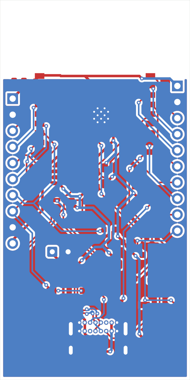
Deliberately arranged so each header carries the module pins physically nearest it. Getting this wrong forces nets across the whole board and makes a 2-layer route impossible without cutting the ground plane.
| J1 (left) | J2 (right) |
|---|---|
| 1 +3V3 · 2 GND | 1 +3V3 · 2 GND |
| 3 IO4 · 4 IO5 · 5 IO6 · 6 IO7 | 3 IO0 · 4 IO1 · 5 IO2 · 6 IO3 |
| 7 IO8 · 8 IO9 | 7 IO21/TX · 8 IO20/RX · 9 IO10 |
| 9 GND · 10 +3V3 | 10 EN |
cp -r examples/esp32c3-devboard /tmp/demo && cd /tmp/demo
../../scripts/preflight.sh beautiful.kicad_pcb
python ../../scripts/verify.py beautiful.kicad_pcb --spec constraints.yaml --sch beautiful.kicad_schmedia/routing.gif - 46 frames replaying the router's own event log
(KICAD_ROUTE_TRACE=1), showing traces laid, ripped and restored. Open it in a
browser; some image viewers show only the first frame.
0 DRC errors, 0 unconnected pads. 5 of 6 TransPCB checks pass.
Placement was refined by place_optimise.py (simulated annealing) and fully
re-routed. Against the hand-placed original:
| hand-placed | optimised | |
|---|---|---|
| copper | 772.4 mm | 661.0 mm |
| vias | 92 | 42 |
| ESP32 3V3 pin to nearest 100 nF | 22.00 mm | 4.09 mm |
| DRC errors | 0 | 0 |
That last row is the one that matters: decoupling 22 mm from the pin it serves
is ornamental. It also drove four fixes in the optimiser - see the
pcb-place skill.
Routed with the two-stage flow - route_diff.py for the USB pair first, then
route.py for the rest. Pair skew: connector side 7.39 -> 3.26 mm, MCU side
13.42 -> 5.16 mm against a single-ended first attempt.
A board-level ANTENNA_KEEPOUT zone (tracks, vias and pour not allowed) keeps
the RF region clear - the router respects it, rather than the verifier catching
intrusions afterwards. Its boundary is y=61.5 rather than the footprint's 61.9,
because U1's own pads sit at y=62.0 and a 0.4 mm track reaching them spans
61.8..62.2.
diffpair:USB - copper skew 2.89 mm against a 2.5 mm threshold
(USB_DP 85.19 mm / 2 vias, USB_DM 82.29 mm / 4 vias).
This is the term that regressed when placement was optimised for decoupling: skew was 1.52 mm before. A deliberate trade, and the right one here - at 12 Mbps full-speed a bit period is 83 ns, and 2.9 mm of FR4 is roughly 19 ps, under 0.03% of a bit. USB 2.0 full speed also has no impedance-matching requirement; that begins at high speed, 480 Mbps.
It would matter on a faster interface or in EMC testing. Fixing it properly means placement work around TP3/TP4 and the ESD part, not re-routing.
| Qty | Value | Footprint | References |
|---|---|---|---|
| 3 | 100nF | C_0603_1608Metric | C1, C5, C7 |
| 3 | 1k | R_0603_1608Metric | R2, R3, R4 |
| 2 | 10uF | C_0805_2012Metric | C2, C4 |
| 2 | 5.1k | R_0603_1608Metric | R7, R8 |
| 1 | 100uF/16V | CP_Radial_D6.3mm_P2.50mm | CP1 |
| 1 | 10k | R_0603_1608Metric | R1 |
| 1 | 1uF | C_0603_1608Metric | C3 |
| 1 | 22uF | C_0805_2012Metric | C6 |
| 1 | 3V3 | TestPoint_Pad_D1.5mm | TP1 |
| 1 | AP2112K-3.3 | SOT-23-5 | U2 |
| 1 | BOOT | Panasonic_EVQPUJ_EVQPUA | SW2 |
| 1 | EN | TestPoint_Pad_D1.5mm | TP6 |
| 1 | ESP32-C3-WROOM-02 | ESP32-C3-WROOM-02 | U1 |
| 1 | GND | TestPoint_Pad_D1.5mm | TP2 |
| 1 | GPIO-A | PinHeader_1x10_P2.54mm_Vertical | J1 |
| 1 | GPIO-B | PinHeader_1x10_P2.54mm_Vertical | J2 |
| 1 | IO10 | LED_0603_1608Metric | D3 |
| 1 | IO8 | LED_0603_1608Metric | D2 |
| 1 | PWR | LED_0603_1608Metric | D1 |
| 1 | RESET | Panasonic_EVQPUJ_EVQPUA | SW1 |
| 1 | USB-C | USB_C_Receptacle_GCT_USB4085 | J3 |
| 1 | USBLC6-2SC6 | SOT-23-6 | U3 |
| 1 | USB_DM | TestPoint_Pad_D1.5mm | TP4 |
| 1 | USB_DP | TestPoint_Pad_D1.5mm | TP3 |
| 1 | VBUS | TestPoint_Pad_D1.5mm | TP5 |
pushtiujeniya/ESP32-C3-WROOM02_dev-board
This project is a custom 2-layer development board designed around the ESP32-C3-WROOM-02 Wi‑Fi + Bluetooth MCU module.


anasskrim61-wq/esp32-c3-mini
Custom ESP32-C3 Mini IoT hardware design and KiCad PCB project

bapsenpai-blip/STM32F405-4-layer-flight-controller
My first PCB revision, not fabricated yet, looking for design review

NozomiNetworks/NN-antenna-manager
Open source project for a custom antenna manager for SDR cards

aayanrahman/Star-Notifier
Star-shaped USB-C ESP32-C3 board that lights up when Claude or Cursor is done

Akshath2002/ESP32-Mini-Evaluation-Board
A compact 4-layer ESP32 evaluation board designed in KiCad, focused on reliable power distribution, signal integrity, and ease of prototyping.

Alexden28/esp32c3-sensor-node-pcb
2-layer ESP32-C3 + SHT40 USB-C sensor node in KiCad 10, generated from Python, autorouted, ERC/DRC clean, with Gerbers/BOM/CPL/STEP
It measures 30 × 60 mm and has 2 copper layers, 1.6 mm thick.
31 parts, built around the ESP32-C3-WROOM-02-H4, AP2112K-3.3, USBLC6-2SC6 and 100UF/16V. The full list of its parts is on this page, with links to each part's symbol and footprint where PCBKit's library has them.
From the Karasik777/TransPCB repository on GitHub, at the commit this page was made from: the board is examples/esp32c3-devboard/beautiful.kicad_pcb and its schematic examples/esp32c3-devboard/beautiful.kicad_sch. PCBKit opens the board in the browser, with nothing to install.
Its repository publishes it under the MIT licence: you may reuse it on that licence's terms (keep the author's notice, and for a copyleft licence share your changes alike).