4 layers80.1 × 22.2 mm
M2-smart iot module
antmicro/m2-smart-iot-module
https://antmicro.com/blog/2021/08/open-hardware-smart-m2-radio-module-for-iot/
212 parts30Apache-2.0

 kaievns/plan-b
Baking the ultimate split BLE keyboard PCB
Plan b is an open-source printed circuit board by kaievns, from the kaievns/plan-b repository on GitHub. It is a 4-layer board of 16 × 42 mm with 65 parts on 102 nets, routed with 751 tracks and 121 vias.
It is built around the NRF52840-QIAA-R and ANT2012LL13R2400A. Its parts include 23 capacitors, 9 connectors, 5 resistors, 4 ICs and 4 switches. It belongs with the keyboards and input and radio and wireless boards and the nRF52 and nRF5x boards of this library.


This is a tiny opinionated PCB that has everything packed in one place for creating split bluetooth keyboards on top of nrf52840 chip and ZMK firmware
Think about it as
All in a tiny 14x42mm package, which is about 8m longer than nice!view shield
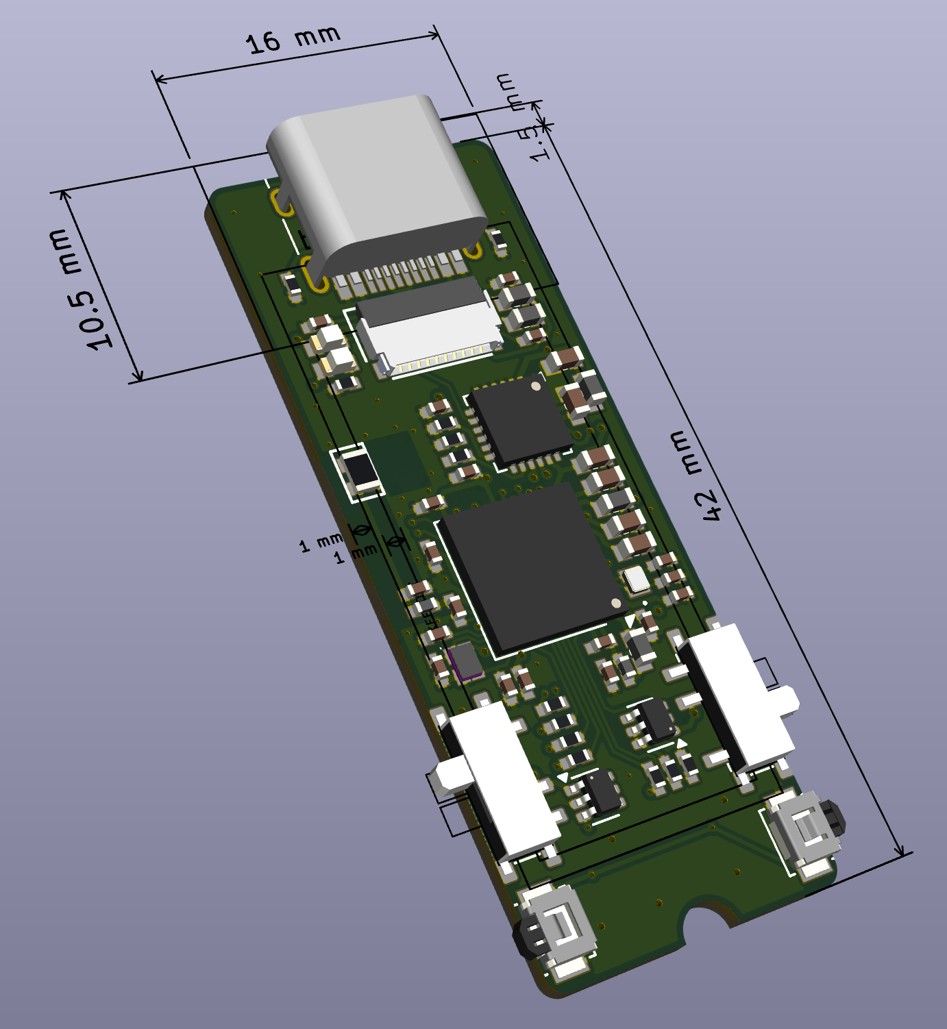
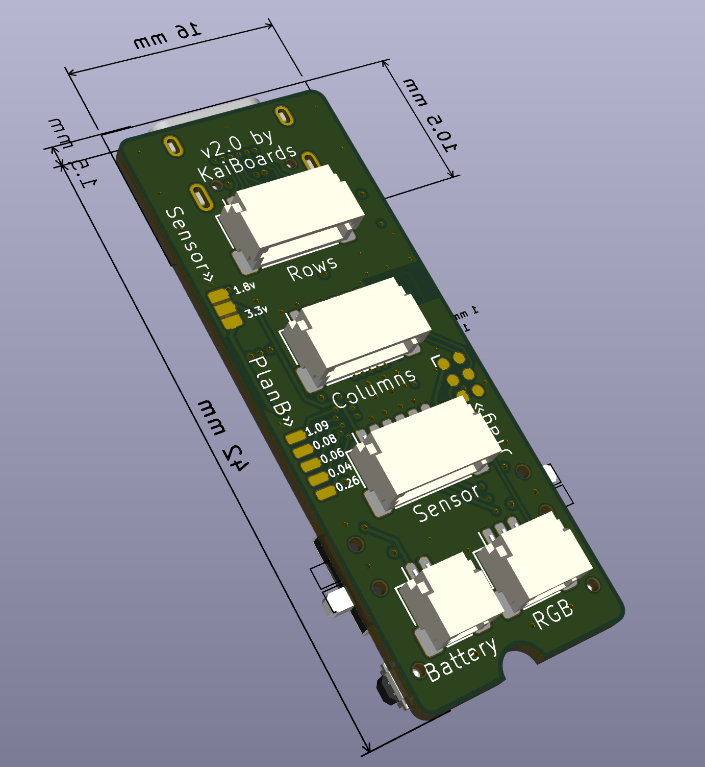
Everything is released under the terms of the CC BY-SA 4.0 license
© 2025 Kai Evans
| Qty | Value | Footprint | References |
|---|---|---|---|
| 5 | 1.0µF | Library:C_0402_1005 | C14, C15, C22, C30, C38 |
| 5 | 100R | Library:R_0402_1005 | R8, R11, R14, R15, R16 |
| 5 | 5k1 | Library:R_0402_1005 | R_ICHG1, R3, R21, R22, R33 |
| 4 | 100k | Library:R_0402_1005 | R_BLE1, R_BLE2, R_DIV1, R_DIV2 |
| 4 | 100nF | Library:C_0402_1005 | C5, C7, C8, C12 |
| 4 | 12pF | Library:C_0402_1005 | C1, C2, C17, C18 |
| 3 | 4.7µF | Library:C_0603_1608 | C6, C20, C21 |
| 2 | 10µH | Library:L_0603_1608 | L2, L4 |
| 2 | 600R | Library:F_0603_1608 | FB1, FB2 |
| 2 | Power | ScottoKeebs_Components:Switch_MSK12C02 | SW1, SW1 |
| 2 | Reset | Button_Switch_SMD:SW_SPST_B3U-3000P-B | SW2, SW2 |
| 2 | TPS22919DCKR | Package_TO_SOT_SMD:SOT-363_SC-70-6 | U3, U4 |
| 1 | 0.5 pF | Library:C_0402_1005 | C4 |
| 1 | 0.8 pF | Library:C_0402_1005 | C3 |
| 1 | 100pF | Library:C_0402_1005 | C11 |
| 1 | 10µF | Library:C_0603_1608 | C19 |
| 1 | 15nH | Library:L_0402_1005 | L3 |
| 1 | 32.768kHz | EXC-1210:XTAL_ECS32761210TR | X2 |
| 1 | 32MHz | NX1612SA-32.000MHZ-CHP:OSCSC105P160X120X35-4N | X1 |
| 1 | 4.7 nH | Library:L_0402_1005 | L1 |
| 1 | 47nF | Library:C_0402_1005 | C16 |
| 1 | 560pF | Library:C_0402_1005 | C37 |
| 1 | 820pF | Library:C_0402_1005 | C9 |
| 1 | ANT2012LL13R2400A | YAGEO Antenna:ANT2012LL13R2400A | AE1 |
| 1 | Battery | Connector_JST:JST_SH_SM02B-SRSS-TB_1x02-1MP_P1.00mm_Horizontal | J2 |
| 1 | Conn_01x05_Pin | Connector_JST:JST_SHL_SM05B-SHLS-TF_1x05-1MP_P1.00mm_Horizontal | J9 |
| 1 | Conn_01x10 | Hirose FH34SRJ-10S-0.5SH:CONN10x1_FH34SRJ-10S-0.5SH50_HIR | J5 |
| 1 | Conn_ARM_SWD_TagConnect_TC2030-NL | Connector:Tag-Connect_TC2030-IDC-NL_2x03_P1.27mm_Vertical | J8 |
| 1 | HRO_TYPE-C-31-M-12 | Connector_USB:USB_C_Receptacle_HRO_TYPE-C-31-M-12 | J1 |
| 1 | L0603 (Blue) | Library:LED_0603_1608 | LD3 |
| 1 | L0603G (Amber) | Library:LED_0603_1608 | LD2 |
| 1 | columns | Connector_JST:JST_SH_SM06B-SRSS-TB_1x06-1MP_P1.00mm_Horizontal | J4 |
| 1 | nPM1100-QDAx | Package_DFN_QFN:QFN-24-1EP_4x4mm_P0.5mm_EP2.6x2.6mm_ThermalVias | U2 |
| 1 | nRF52840-QIAA | Package_DFN_QFN:Nordic_AQFN-73-1EP_7x7mm_P0.5mm | U1 |
| 1 | rgb | Connector_JST:JST_SH_SM03B-SRSS-TB_1x03-1MP_P1.00mm_Horizontal | J3 |
| 1 | rows | Connector_JST:JST_SH_SM06B-SRSS-TB_1x06-1MP_P1.00mm_Horizontal | J6 |
| 1 | sensor | Connector_JST:JST_SH_SM06B-SRSS-TB_1x06-1MP_P1.00mm_Horizontal | J7 |
It measures 16 × 42 mm and has 4 copper layers, 1.14 mm thick.
65 parts, built around the NRF52840-QIAA-R and ANT2012LL13R2400A. The full list of its parts is on this page, with links to each part's symbol and footprint where PCBKit's library has them.
From the kaievns/plan-b repository on GitHub, at the commit this page was made from: the board is plan-b.kicad_pcb and its schematic io.kicad_sch. PCBKit opens the board in the browser, with nothing to install.
Its repository states no licence, so its author keeps all rights: ask kaievns before reusing the design.
antmicro/m2-smart-iot-module
https://antmicro.com/blog/2021/08/open-hardware-smart-m2-radio-module-for-iot/

tiacsys/ecad-coffeecaller
CoffeeCaller. Once a nice office gadget it now evolved to a small development board for the Nordic nRF52840.

jayis1/hacker-devices
Full-cycle hardware designs for security research devices — each device is a subfolder with its own README, schematics, PCB layout, and software stack


anivelle/drone-controller
My attempt at making a drone flight controller. (On hold until I can debug my DShot with an oscilloscope)