2 layers100 × 60 mm

 m5kro/KiKard-old1
Non working project
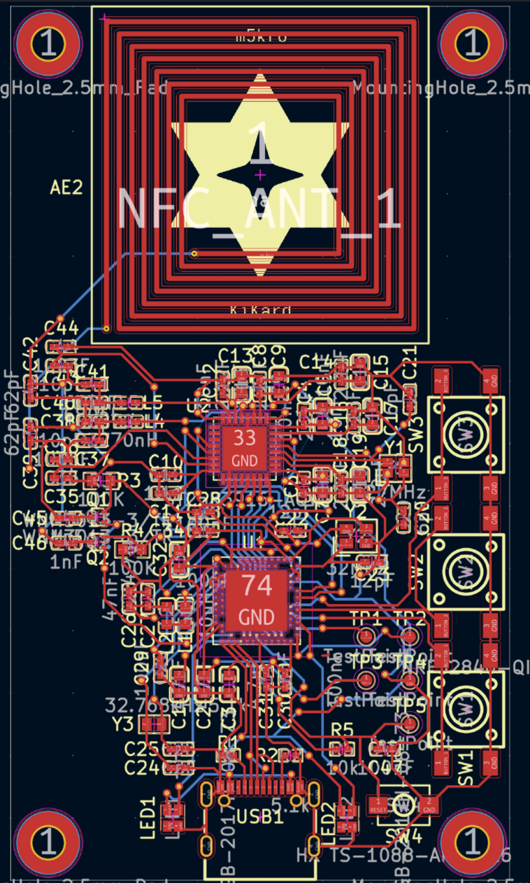
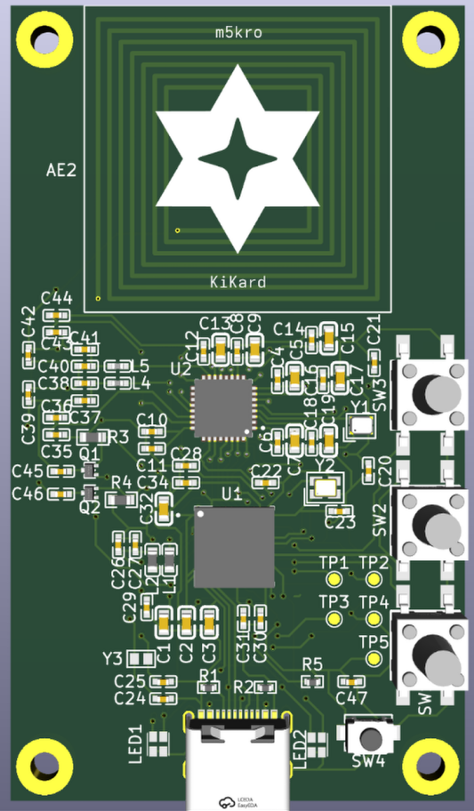
Kikard is an open-source printed circuit board by m5kro, from the m5kro/KiKard-old repository on GitHub. It is a 2-layer board of 40 × 70 mm with 80 parts on 95 nets, routed with 722 tracks and 102 vias.
It is built around the NRF52840-QIAA-R, ST25R3916-AQWT and K2-6639SP-C4SC-04, with the WNM3013-3/TR, ZSRGB-2017H-08-Z3 and TYPE-C16PIN among its other parts. Its parts include 46 capacitors, 5 resistors, 4 switches, 4 inductors and 3 crystals. It belongs with the nRF52 and nRF5x boards of this library.


KiKard is a non working attempt at creating an NFC testing device. This repo is just here as an example for what not to do.
There will be a v2 of the project where I fix my mistakes, lower the costs, and make some general improvements.
Here's a medium article explaining what went wrong: Here
Here's what it looks like:
| Qty | Value | Footprint | References |
|---|---|---|---|
| 8 | 10nF | extra-symbols-footprints:C0402 | C4, C6, C8, C10, C12, C14, C16, C18 |
| 7 | 2.2uF | extra-symbols-footprints:C0603 | C5, C7, C9, C13, C15, C17, C19 |
| 6 | 100nF | extra-symbols-footprints:C0402 | C28, C29, C30, C31, C34, C47 |
| 5 | TestPoint | extra-symbols-footprints:TestPoint_Pad_D1.0mm | TP1, TP2, TP3, TP4, TP5 |
| 4 | 100pF | extra-symbols-footprints:C0402 | C35, C37, C41, C44 |
| 4 | 4.7uF | extra-symbols-footprints:C0603 | C1, C2, C3, C32 |
| 4 | 6pF | extra-symbols-footprints:C0402 | C20, C21, C24, C25 |
| 3 | K2-6639SP-C4SC-04 | extra-symbols-footprints:KEY-SMD_4P-L6.0-W6.0-P3.90-LS9.0 | SW1, SW2, SW3 |
| 2 | 100K | extra-symbols-footprints:R0603 | R3, R4 |
| 2 | 10pF | extra-symbols-footprints:C0402 | C36, C43 |
| 2 | 12pF | extra-symbols-footprints:C0402 | C22, C23 |
| 2 | 1nF | extra-symbols-footprints:C0402 | C45, C46 |
| 2 | 1uF | extra-symbols-footprints:C0402 | C11, C27 |
| 2 | 270nH | extra-symbols-footprints:L0402 | L4, L5 |
| 2 | 5.1k | extra-symbols-footprints:R0402 | R1, R2 |
| 2 | 62pF | extra-symbols-footprints:C0402 | C39, C42 |
| 2 | 680pF | extra-symbols-footprints:C0402 | C38, C40 |
| 2 | WNM3013-3/TR | extra-symbols-footprints:SOT-723_L1.2-W0.8-P0.40-LS1.2-BR | Q1, Q2 |
| 2 | ZSRGB-2017H-08-Z3 | extra-symbols-footprints:LED-SMD_4P-L2.0-W1.8-P0.90_XGM-S0807RGB | LED1, LED2 |
| 1 | 10k | extra-symbols-footprints:R0402 | R5 |
| 1 | 10uH | extra-symbols-footprints:L0603 | L1 |
| 1 | 15nH | extra-symbols-footprints:L0603 | L2 |
| 1 | 27MHz | extra-symbols-footprints:CRYSTAL-SMD_4P-L2.0-W1.6-BL-B | Y1 |
| 1 | 32.768kHz | extra-symbols-footprints:OSC-SMD_L1.6-W1.0 | Y3 |
| 1 | 32MHz | extra-symbols-footprints:CRYSTAL-SMD_4P-L2.0-W1.6-BL-2 | Y2 |
| 1 | 47nF | extra-symbols-footprints:C0402 | C26 |
| 1 | Antenna_Loop | extra-symbols-footprints:kikard-ant-v1.0 | AE2 |
| 1 | HX TS-1088-AR02016 | extra-symbols-footprints:SW-SMD_L4.0-W2.9-LS5.0 | SW4 |
| 1 | LOGO | extra-symbols-footprints:logo | G*** |
| 1 | NRF52840-QIAA-R | extra-symbols-footprints:XCVR_NRF52840-QIAA-R | U1 |
| 1 | ST25R3916-AQWT | extra-symbols-footprints:QFN50P500X500X100-33N | U2 |
| 1 | TYPE-C16PIN | extra-symbols-footprints:USB-C-SMD_TYPE-C16PIN | USB1 |
The 76 most common of 80 parts.

Volkov997/pen-card
RF Pentesting tool, but small enough for your wallet. Features: Wifi & Bluetooth, NFC, IR, (Sub Ghz, Planned)


rajinthanr/attendance-management-system
Battery-powered NFC attendance logger (STM32L432 + ST25R3916) that mounts as a USB drive, with a Qt companion app

rabinniroula/tapper-hw
KiCad Design Files for Tapper: A hardware tool for LF and HF RFID read, emulation and much more...

antmicro/m2-smart-iot-module
https://antmicro.com/blog/2021/08/open-hardware-smart-m2-radio-module-for-iot/

tiacsys/ecad-coffeecaller
CoffeeCaller. Once a nice office gadget it now evolved to a small development board for the Nordic nRF52840.

jayis1/hacker-devices
Full-cycle hardware designs for security research devices — each device is a subfolder with its own README, schematics, PCB layout, and software stack
It measures 40 × 70 mm and has 2 copper layers, 1.6 mm thick.
80 parts, built around the NRF52840-QIAA-R, ST25R3916-AQWT, K2-6639SP-C4SC-04 and WNM3013-3/TR. The full list of its parts is on this page, with links to each part's symbol and footprint where PCBKit's library has them.
From the m5kro/KiKard-old repository on GitHub, at the commit this page was made from: the board is hardware/kikard.kicad_pcb and its schematic hardware/kikard.kicad_sch. PCBKit opens the board in the browser, with nothing to install.
Its repository states no licence, so its author keeps all rights: ask m5kro before reusing the design.