2 layers30.5 × 68.6 mm

 jvanderberg/pico-stretch22
An RP2350B dev board that breaks out all 48 GPIO pins while following the original Raspberry Pi Pico footprint for the first 20 pins on each side.
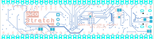
Pico stretch2 is an open-source printed circuit board by jvanderberg, from the jvanderberg/pico-stretch2 repository on GitHub. It is a 4-layer board of 82.1 × 21 mm with 70 parts on 93 nets, routed with 880 tracks and 234 vias.
It is built around the W25Q128JVSIQ TR, APS6404L-3SQR-SN and ME6217C33M5G, with the K2-1808SN-A4SW-01, AOTA-B201610S3R3-101-T and KT-0603R among its other parts. Its parts include 27 capacitors, 16 resistors, 5 ICs, 3 diodes and 2 connectors. It belongs with the RP2040 and RP2350 boards of this library.


An RP2350B dev board that breaks out all 48 GPIO pins while following the original Raspberry Pi Pico footprint for the first 20 pins on each side. It adds another 12 pins on each side — keeping the same 0.1" pitch and castellated edges so it remains breadboard-friendly.
The board supports PSRam (chip select on GP0 or GP47) and the Radio Module 2 for WiFi/BT
Features:
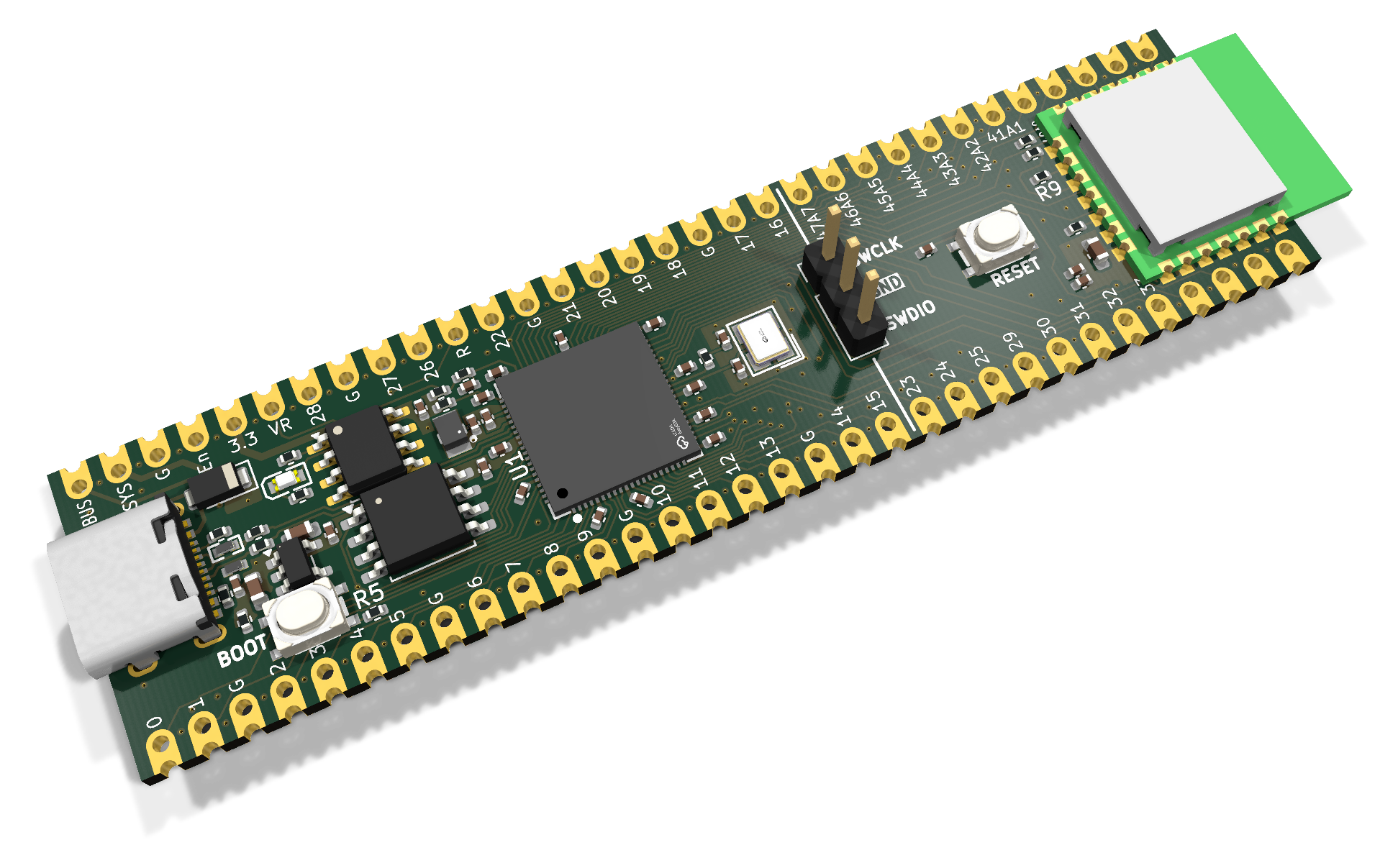
Top
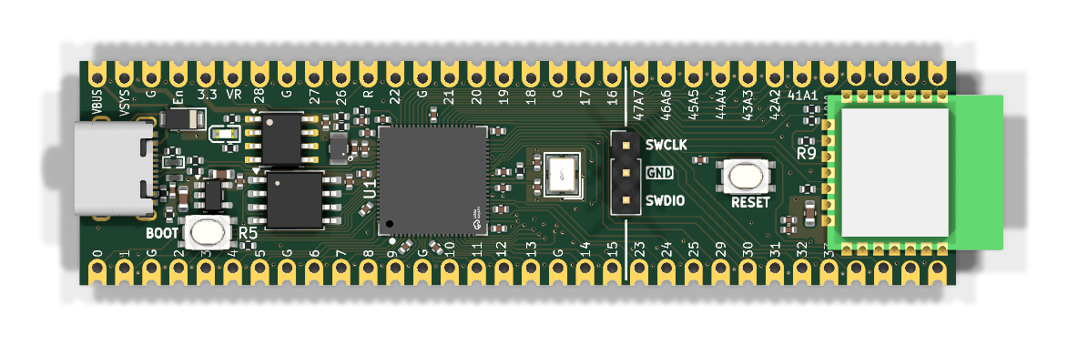
Bottom
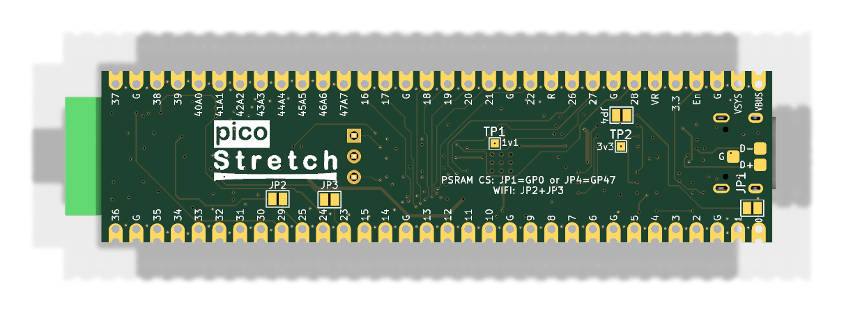
F.Cu / F.Silkscreen
B.Cu / B.Silkscreen (mirrored)
1   GPIO0           64  VBUS
2   GPIO1           63  VSYS
3   GND             62  GND
4   GPIO2           61  3v3_EN
5   GPIO3           60  3v3
6   GPIO4           59  ADC_VREF
7   GPIO5           58  GPIO28
8   GND             57  GND
9   GPIO6           56  GPIO27
10  GPIO7           55  GPIO26
11  GPIO8           54  RUN
12  GPIO9           53  GPIO22
13  GND             52  GND
14  GPIO10          51  GPIO21
15  GPIO11          50  GPIO20
16  GPIO12          49  GPIO19
17  GPIO13          48  GPIO18
18  GND             47  GND
19  GPIO14          46  GPIO17
20  GPIO15          45  GPIO16
21  GPIO23          44  GPIO47/ADC7
22  GPIO24          43  GPIO46/ADC6
23  GPIO25          42  GPIO45/ADC5
24 GPIO29 41 GPIO44/ADC4PICO_FLASH_SPI_CLKDIV 2. If you see flash or PSRAM errors at higher system clocks, use a larger
divider (4) and test before going back down.The first 20 castellated pads on each side, and the USB test pads above, line up with the Raspberry Pi Pico / Pico 2 SMT footprint (Pico 2 datasheet section 3.2), so the board can be hot-plate or reflow soldered onto a carrier designed for a Pico. The other 24 pads and the radio end overhang the Pico outline.
Production files live in the production/ directory, written by
JLCImport's jlcimport-cli production from the board as it is:
pico-stretch2-gerbers.zip — Gerber and drill files (the same files, unzipped, are in gerbers/)pico-stretch2-bom.csv — bill of materialspico-stretch2-cpl.csv — component placement file, with rotations solved against JLC's own footprintspico-stretch2-report.txt — the production check: stock, part types, fees, and the placements to look at in
JLC's previewTo regenerate after a board change: jlcimport-cli production pico-stretch2.kicad_pcb (add --force to write
the files even when the check reports an error, such as a part out of stock).
When ordering:
Run scripts/render-images.sh after PCB changes to regenerate everything in images/. Requires kicad-cli (KiCad ≥ 9) and ImageMagick (magick).
| Qty | Value | Footprint | References |
|---|---|---|---|
| 15 | 100nF | Capacitor_SMD:C_0402_1005Metric | C1, C3, C4, C5, C6, C7, C8, C9, C13, C15, C16, C21, C22, C23, C36 |
| 5 | 4.7uF | Capacitor_SMD:C_0402_1005Metric | C2, C10, C11, C12, C19 |
| 4 | SolderJumper_2_Open | Jumper:SolderJumper-2_P1.3mm_Open_Pad1.0x1.5mm | JP1, JP2, JP3, JP4 |
| 3 | 10kΩ | Resistor_SMD:R_0402_1005Metric | R9, R10, R16 |
| 3 | 1kΩ | Resistor_SMD:R_0402_1005Metric | R5, R14, R28 |
| 3 | 33Ω | Resistor_SMD:R_0402_1005Metric | R2, R3, R6 |
| 3 | TestPoint | Custom:TestPoint_Pad_1.5x1.5mm_R0.3mm | TP3, TP4, TP5 |
| 2 | 10uF | Capacitor_SMD:C_0603_1608Metric | C37, C40 |
| 2 | 15pF | Capacitor_SMD:C_0402_1005Metric | C17, C18 |
| 2 | 5.1kΩ | Resistor_SMD:R_0402_1005Metric | R1, R4 |
| 2 | CL05B104KO5NNNC | Capacitor_SMD:C_0402_1005Metric | C38, C39 |
| 2 | K2-1808SN-A4SW | EasyEDA:K2-1808SN-A4SW | Boot1, Reset1 |
| 2 | RCLAMP0521P_TCT_C3029033 | EasyEDA:RCLAMP0521P_TCT_C3029033 | D2, D3 |
| 2 | TestPoint | TestPoint:TestPoint_Pad_1.0x1.0mm | TP1, TP2 |
| 1 | 100kΩ | Resistor_SMD:R_0402_1005Metric | R11 |
| 1 | 1Ω | Resistor_SMD:R_0402_1005Metric | R7 |
| 1 | 200Ω | Resistor_SMD:R_0402_1005Metric | R8 |
| 1 | 2kΩ | Resistor_SMD:R_0402_1005Metric | R12 |
| 1 | 470Ω | Resistor_SMD:R_0402_1005Metric | R15 |
| 1 | ABM8-272-T3_C20625731 | EasyEDA:ABM8-272-T3_C20625731 | X1 |
| 1 | AOTA-B201610S3R3-101-T | EasyEDA:AOTA-B201610S3R3-101-T | L1 |
| 1 | APS6404L-3SQR | Package_SO:SOIC-8_3.9x4.9mm_P1.27mm | U6 |
| 1 | CL10A475KO8NNNC | Capacitor_SMD:C_0603_1608Metric | C24 |
| 1 | Conn_01x03_Pin | Connector_PinHeader_2.54mm:PinHeader_1x03_P2.54mm_Vertical | J2 |
| 1 | Conn_01x64_Castellated_Pads | Castellated:Castellated_Pad_64 | J4 |
| 1 | DFLS130L-7 | Diode_SMD:D_PowerDI-123 | D1 |
| 1 | KT-0603R | EasyEDA:KT-0603R | PWR_LED1 |
| 1 | LOGO | Custom:logo | G*** |
| 1 | LOGO | Custom:logo_large | G*** |
| 1 | ME6217C33M5G | Package_TO_SOT_SMD:SOT-23-5 | U3 |
| 1 | RP2350B_C42415655 | EasyEDA:RP2350B_C42415655 | U1 |
| 1 | RPI Radio Module 2 | Custom:rpi_rmc20452t | U5 |
| 1 | TYPE-C_16PIN_2MD_073 | EasyEDA:TYPE-C_16PIN_2MD_073 | USB1 |
| 1 | W25Q128JVSIQTR | Package_SO:SOIC-8_5.3x5.3mm_P1.27mm | U4 |
It measures 82.1 × 21 mm and has 4 copper layers, 1.6 mm thick.
70 parts, built around the W25Q128JVSIQ TR, APS6404L-3SQR-SN, ME6217C33M5G and K2-1808SN-A4SW-01. The full list of its parts is on this page, with links to each part's symbol and footprint where PCBKit's library has them.
From the jvanderberg/pico-stretch2 repository on GitHub, at the commit this page was made from: the board is pico-stretch2.kicad_pcb and its schematic pico-stretch2.kicad_sch. PCBKit opens the board in the browser, with nothing to install.
Its repository states no licence, so its author keeps all rights: ask jvanderberg before reusing the design.


thejamesrhodes/Hyades-Flight-Computer
Full Hardware and Electronics design, Bare-metal GNC flight software for an actively attitude-controlled high-power rocket


enkhbold470/ice-core
iCE40UP5K FPGA board with 8 MB PSRAM and three Pmods, programmed over USB-C by an RP2040. 6-layer KiCad 10 board.