
4 layers111 × 171 mm
Network and Switch
AkshathRaghav/boilernet
Code release for BoilerNet, demo'd at SPARK S'25 as a Purdue Senior Design Capstone. Associated PCB Design and 3D Prints within.
108 parts3Apache-2.0

Full-size mechanical keyboard with USB-C and no lighting.
JayK is an open-source printed circuit board by josuegaleas, from the josuegaleas/JayK repository on GitHub, published under the Apache-2.0 licence. It is a 2-layer board of 419.1 × 101.2 mm with 207 parts on 134 nets, routed with 1,427 tracks and 31 vias.
It is built around the AT90USB1286-AU and PESD5V0L2BT. Its parts include 94 diodes, 94 switches, 1 IC, 1 connector and 1 crystal. It belongs with the keyboards and input boards and the AVR (ATmega, ATtiny) boards of this library.


Full-size mechanical keyboard with USB-C and no lighting, inspired by the ONO-SENDAI MATRIX 83.
JayK Pro with more features can be found here.
I have not printed this PCB out yet, and I am not 100% certain the design works. Please print with discretion.
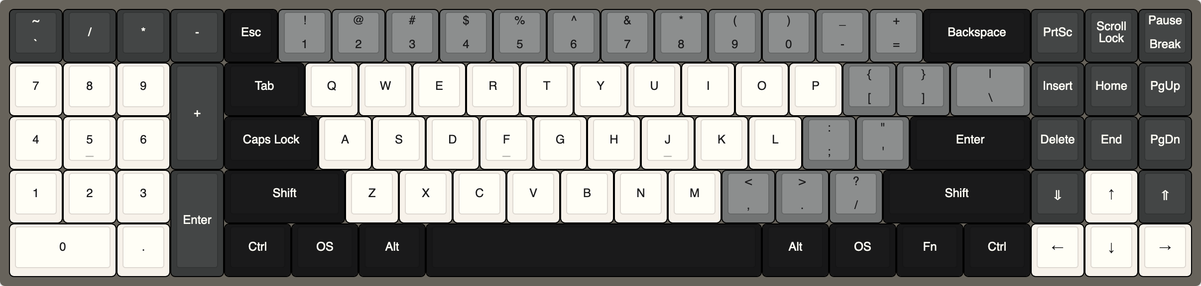
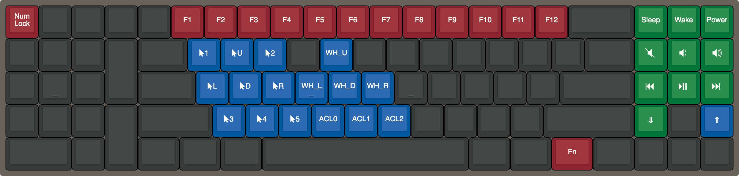
JSON files for these layouts can be found here and here, for editing in KLE.
Clone this repository with:
git clone --recursive https://github.com/josuegaleas/JayK.gitWithin KiCad, navigate to the PCB folder and open JayK.pro.
Using a grid size of 0.0234375 inches for editing the layout.
Firmware can be compiled using make within the Firmware folder.
Refer to this for dependencies and programming.
| Qty | Value | Footprint | References |
|---|---|---|---|
| 94 | D | keyboard_parts:D_SOD123_axial | D0,0, D0,1, D0,2, D0,3, D0,4, D0,10, D0,11, D0,12, D0,13, D0,14, D0,15, D0,16, D0,17, D0,18, D0,19, D0,20 +78 |
| 75 | KEYSW | keebs:Mx_Alps_100 | K0,0, K0,1, K0,2, K0,3, K0,4, K0,5, K0,10, K0,11, K0,12, K0,13, K0,14, K0,15, K0,16, K0,18, K0,19, K0,20 +59 |
| 7 | KEYSW | keebs:Mx_Alps_125 | K4,4, K4,5, K4,6, K4,13, K4,14, K4,16, K4,17 |
| 5 | 100n | Capacitor_SMD:C_0805_2012Metric_Pad1.15x1.40mm_HandSolder | C_AREF1, C_AVCC1, C_UVCC1, C_VCC1, C_VCC2 |
| 4 | KEYSW | keebs:Mx_Alps_200 | K0,17, K1,3, K3,3, K4,0 |
| 2 | 22 | Resistor_SMD:R_0805_2012Metric_Pad1.15x1.40mm_HandSolder | R_USB1, R_USB2 |
| 2 | 22p | Capacitor_SMD:C_0805_2012Metric_Pad1.15x1.40mm_HandSolder | C_CLK1, C_CLK2 |
| 2 | 5.1k | Resistor_SMD:R_0805_2012Metric_Pad1.15x1.40mm_HandSolder | R_USB3, R_USB4 |
| 2 | KEYSW | keebs:Mx_Alps_150 | K1,4, K1,17 |
| 2 | KEYSW | keebs:Mx_Alps_225 | K2,17, K3,4 |
| 1 | 10u | Capacitor_SMD:C_0805_2012Metric_Pad1.15x1.40mm_HandSolder | C_VBUS1 |
| 1 | 16M | Crystal:Crystal_SMD_SeikoEpson_FA238-4Pin_3.2x2.5mm_HandSoldering | Y1 |
| 1 | 1k | Resistor_SMD:R_0805_2012Metric_Pad1.15x1.40mm_HandSolder | R_HWB1 |
| 1 | 1u | Capacitor_SMD:C_0805_2012Metric_Pad1.15x1.40mm_HandSolder | C_UCAP1 |
| 1 | 47k | Resistor_SMD:R_0805_2012Metric_Pad1.15x1.40mm_HandSolder | R_RST1 |
| 1 | AT90USB1286-AU | Package_QFP:TQFP-64_14x14mm_P0.8mm | U1 |
| 1 | KEYSW | keebs:Mx_Alps_175 | K2,4 |
| 1 | KEYSW | keebs:Mx_Alps_625 | K4,9 |
| 1 | KEYSW | keebs:Mx_Alps_275 | K3,16 |
| 1 | PESD5V0L2BT | Package_TO_SOT_SMD:SOT-23_Handsoldering | D_ESD1 |
| 1 | SW_PUSH | Button_Switch_SMD:SW_SPST_TL3342 | SW1 |
| 1 | USB_C_Receptacle_USB2.0 | Connector_USB:USB_C_Receptacle_Amphenol_12401610E4-2A | J1 |
AkshathRaghav/boilernet
Code release for BoilerNet, demo'd at SPARK S'25 as a Purdue Senior Design Capstone. Associated PCB Design and 3D Prints within.

lhr-solar/PS-BPSLeader
Reads voltage, temperature, and current of the main battery pack from the Segment Monitoring Board and HV Carrier boards to ensure the battery remains in a safe state.


It measures 419.1 × 101.2 mm and has 2 copper layers, 1.6 mm thick.
207 parts, built around the AT90USB1286-AU and PESD5V0L2BT. The full list of its parts is on this page, with links to each part's symbol and footprint where PCBKit's library has them.
From the josuegaleas/JayK repository on GitHub, at the commit this page was made from: the board is PCB/JayK.kicad_pcb. PCBKit opens the board in the browser, with nothing to install.
Its repository publishes it under the Apache-2.0 licence: you may reuse it on that licence's terms (keep the author's notice, and for a copyleft licence share your changes alike).