CoilTile
jonahsaunders/planar-studio
KiCad extension for the copper you can't buy as a part — design planar inductors, transformers, PCB motor stators, filters, and antennas, with electrical modeling and direct write-back to your board.

KiCad extension for the copper you can't buy as a part — design planar inductors, transformers, PCB motor stators, filters, and antennas, with electrical modeling and direct write-back to your board.
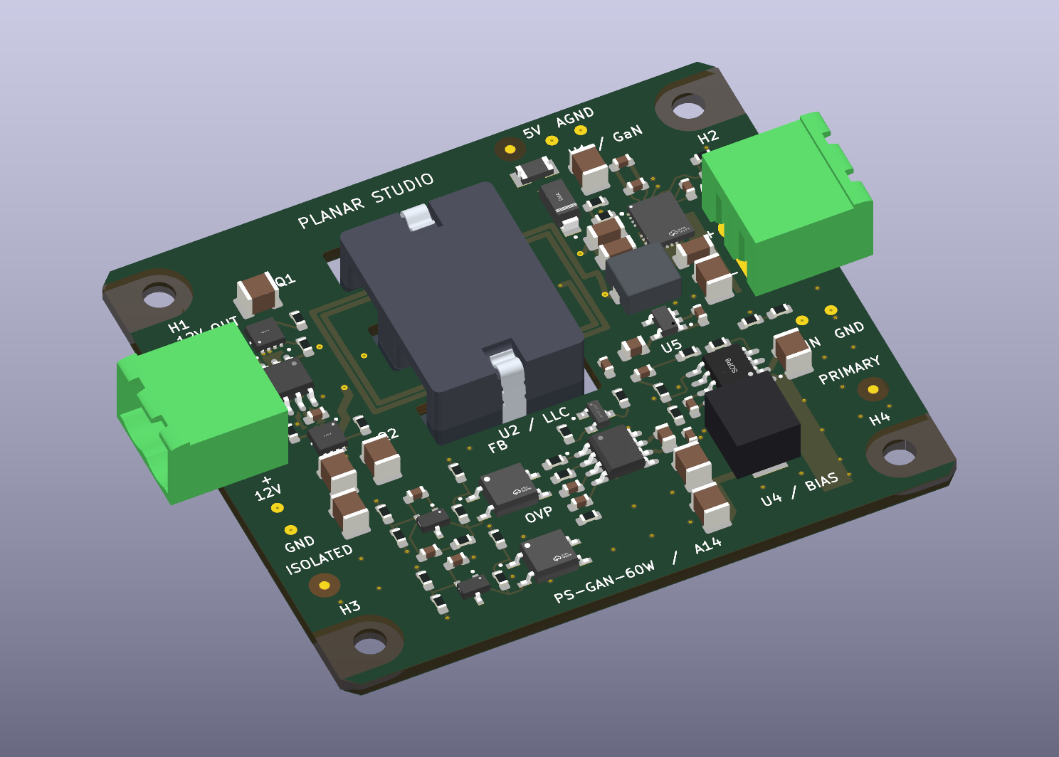
PS GAN-60W is an open-source printed circuit board by jonahsaunders, from the jonahsaunders/planar-studio repository on GitHub, published under the MIT licence. It is an 8-layer board of 64 × 56 mm with 89 parts on 56 nets, routed with 497 tracks and 198 vias.
It is built around the LM5164DDAR, LMG2100R044RARR and UCC24624D, with the UCC25600D, EL357N(A)(TA)-VG and TL431AIDBZR among its other parts. Its parts include 29 capacitors, 28 resistors, 9 ICs, 2 diodes and 2 transistors. It belongs with the radio and wireless and robots and motor control boards of this library.
Design planar inductors, transformers, PCB motors, filters and antennas inside KiCad. Planar Studio reads your board's stack, calculates electrical estimates, and places the generated copper into the PCB as one undoable operation.
Download v1.6.0 · Install · Guides · Common PCB issues · Flyback example · GaN example · CoilTile example
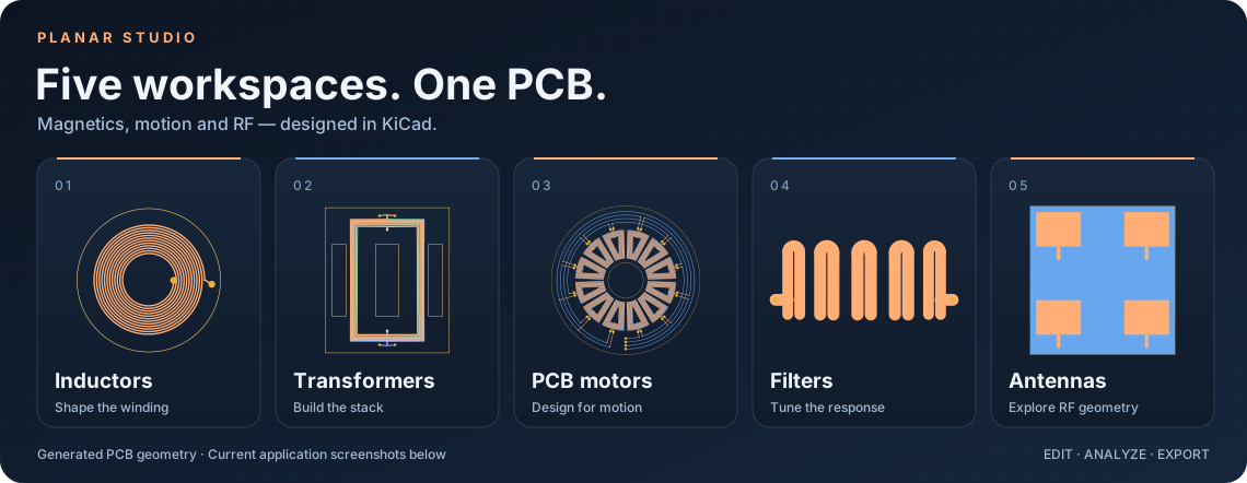
Current application captures. Click a view to open the full-size image.
Inductors
Shape windings, connect layers and route around obstacles. |
Transformers
Build ferrite stacks, compare candidates and verify operating limits. |
PCB motors
Explore rotary, stepper, linear, dual-rotor and planar machines. |
Filters
Turn LC and microstrip networks into copper and response plots. |
Antennas
Design patches, arrays, directional radiators and NFC loops. |
Design tools
Inspect fields, optimize geometry and compare measurements. |
Open the full 15-image gallery → — obstacle routing, transformer search, motor families, antenna variants and both interface themes.
Save editable designs, compare calculated responses, and export KiCad boards or footprints, SVG, DXF, JSON and specification sheets. The Design tools panel adds constrained searches, measurement overlays, tolerance studies and board checks; see the tools guide.
The 1.6.0 development release supports KiCad 9.0.1 or newer on Windows, macOS and Linux. Release notes.
To upgrade, close Planar Studio and the PCB Editor. In Plugin and Content Manager → Installed, uninstall the old version and apply pending changes before installing the new ZIP. Saved designs are stored separately; preserve the settings folder.
Use the installer linked above. GitHub's Code → Download ZIP and Source code archives contain the repository, not a PCM installer.
A10 retains the winding-short repair, increases measured turn gaps to about 0.289 mm, enlarges T1 annular rings and removes tangent secondary-via contacts. Independent geometry, connection-width and full copper/mask Gerber checks protect these changes. Use the A10 package and the common PCB issues reference when reviewing or editing the design.
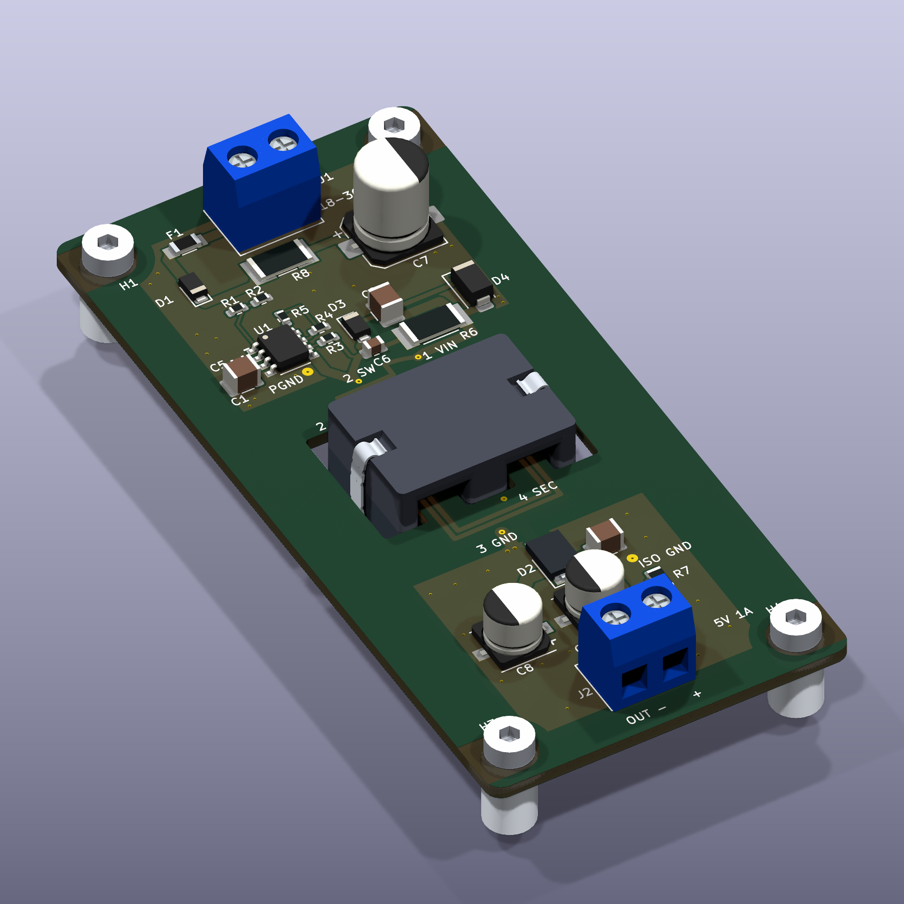
An 18–36 V DC to isolated 5 V / 1 A converter with an LT8302 controller and transformer windings built into a six-layer PCB. The example includes a KiCad 10 project, schematic, BOM, calculations and single-board manufacturing files for JLCPCB-managed panelization.
Unbuilt engineering prototype. Factory acceptance and electrical, thermal and magnetic qualification remain open.
Explore the board and schematic · Review package · Validation record
A 48 V nominal to isolated 12 V / 5 A target using an integrated GaN half bridge, silicon synchronous rectifiers and an eight-layer PCB transformer. The 64 × 56 mm chamfered board has all electronics on top, removable screw-terminal ports, and the flyback example's exposed-substrate M3 hole geometry on a 55 × 47 mm pattern. The A10 schematic uses visible local wiring and has no four-way connections. The accompanying MIT PER and video studies explain the layout decisions. An 82-reference ratings audit records the corrected parts and outstanding electrical limits.
Unbuilt engineering prototype. ERC, DRC, connectivity, assembly-file agreement and a portable rebuild pass. Factory DFM, ferrite installation and electrical, magnetic and thermal qualification remain open. 60 W is not a measured result.
Manufacturing audit: do not order the current revision. The five-board review found overlapping same-net component lands, incomplete courtyards, GaN stencil/mask and placement-origin issues, and a factory stack mismatch. The audit and cost breakdown record required corrections and unconfirmed turnkey operations.
Explore the native KiCad example · KiCad package · Layout resource review · PER design study · Validation record
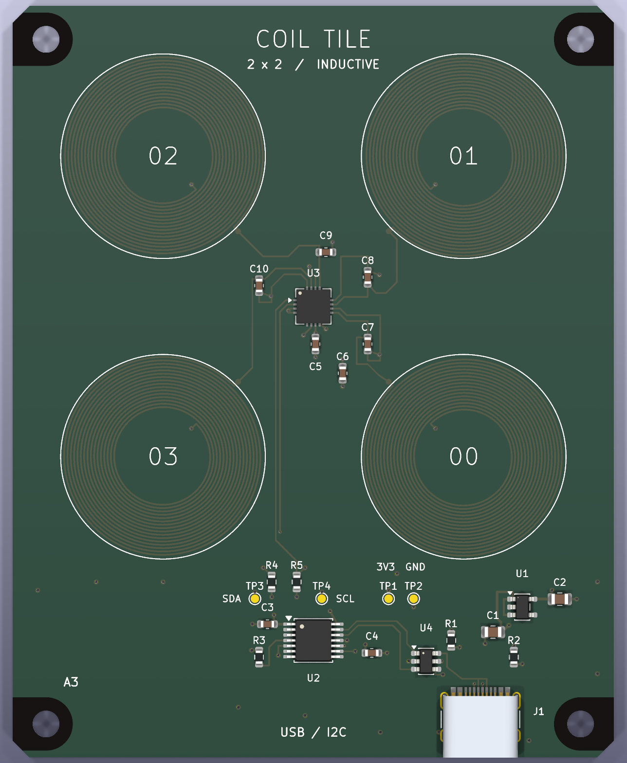
A 2 × 2 near-field metal-sensing array using four printed coils generated by Planar Studio, an LDC1614 converter and an MCP2221A USB bridge. The A3 schematic shows one continuous USB → I²C → sensor → LC-tank signal path. The 72 × 90 mm four-layer PCB reuses the flyback/GaN examples' exposed-substrate M3 edge holes.
Includes editable KiCad 9 files, a Python heatmap and CSV logger, an exact-code JLCPCB BOM/CPL, Gerbers, and bring-up instructions. No firmware flashing is needed. Unbuilt prototype: native ERC/DRC and connectivity checks pass; physical sensing range, crosstalk and supplier assembly acceptance remain unverified.
Explore CoilTile · Schematic PDF · A3 review · Assembly handoff
Calculated performance depends on the selected model. Review its assumptions and validate the resulting hardware with appropriate simulation, KiCad DRC and measurements. Transformer loss or thermal results that cannot be calculated are reported as unknown.
Built on planar-coil-studio. Released under the MIT license.
| Qty | Value | Footprint | References |
|---|---|---|---|
| 6 | 22uF | PS:C_1210_3225Metric | C13, C14, C15, C16, C21, C22 |
| 4 | 10kR | PS:R_0603_1608Metric | R15, R23, R24, R28 |
| 4 | 10nF | PS:C_0603_1608Metric | C17, C18, C27, C29 |
| 4 | 1kR | PS:R_0603_1608Metric | R5, R7, R21, R26 |
| 4 | M3 / NPTH 3.2mm | PS:MountingHole_3.2mm_M3_ExposedSubstrate_Edge | H1, H2, H3, H4 |
| 3 | 100nF | PS:C_0603_1608Metric | C4, C6, C9 |
| 3 | 100nF | PS:C_1206_3216Metric | C3, C7, C8 |
| 3 | 1uF | PS:C_0603_1608Metric | C5, C12, C25 |
| 3 | 2.21kR | PS:R_0603_1608Metric | R4, R6, R9 |
| 3 | 2.2uF | PS:C_1210_3225Metric | C1, C2, C19 |
| 3 | Fiducial_1mm_Mask3mm | PS:Fiducial_1mm_Mask3mm | FID1, FID2, FID3 |
| 2 | 0R | PS:R_0603_1608Metric | R12, R13 |
| 2 | 1.5kR | PS:R_0603_1608Metric | R20, R25 |
| 2 | 2.2R | PS:R_0603_1608Metric | R10, R11 |
| 2 | 2.2uF | PS:C_0805_2012Metric | C11, C26 |
| 2 | 453kR | PS:R_0603_1608Metric | R17, R19 |
| 2 | CSD18543Q3A | PS:VSONP-8_L3.1-W3.1-P0.65-LS3.5-BL | Q1, Q2 |
| 2 | EL357N | PS:OPTO-SMD-4_L4.4-W4.1-P2.54-LS7.0-BL | U6, U8 |
| 2 | TL431A | PS:SOT-23-3_L2.9-W1.6-P1.90-LS2.8-BR | U7, U9 |
| 1 | 1.69kR | PS:R_0603_1608Metric | R2 |
| 1 | 100kR | PS:R_0603_1608Metric | R16 |
| 1 | 12 V / 5 A | PS:CONN-TH_2P-P5.08_WJ2EDGRC-5.08-2P | J2 |
| 1 | 1nF | PS:C_0603_1608Metric | C28 |
| 1 | 1uF | PS:C_0805_2012Metric | C10 |
| 1 | 2.2nF | PS:C_0603_1608Metric | C20 |
| 1 | 24.9kR | PS:R_0603_1608Metric | R8 |
| 1 | 249kR | PS:R_0603_1608Metric | R14 |
| 1 | 3.3kR | PS:R_0603_1608Metric | R1 |
| 1 | 3.3nF | PS:C_0603_1608Metric | C23 |
| 1 | 3.3uH | PS:L_Bourns_SRP5030T | L1 |
| 1 | 38.3kR | PS:R_0603_1608Metric | R22 |
| 1 | 3A / 65V | PS:F1206 | F1 |
| 1 | 4 : 2 : 2 / ELP22 | PS:Planar_ELP22_4_2_2 | T1 |
| 1 | 43.2kR | PS:R_0603_1608Metric | R27 |
| 1 | 48 V INPUT | PS:CONN-TH_2P-P5.08_WJ2EDGRC-5.08-2P | J1 |
| 1 | 49.9kR | PS:R_0603_1608Metric | R18 |
| 1 | 56pF | PS:C_0603_1608Metric | C24 |
| 1 | 68uH | PS:L_Bourns_SRP7050TA | L2 |
| 1 | 750R | PS:R_0603_1608Metric | R3 |
| 1 | AGND | PS:Probe_ENIG_1.2mm | TP6 |
| 1 | BAT54S | PS:SOT-23_L2.9-W1.3-P1.90-LS2.4-BR | D2 |
| 1 | LM5164 | PS:SO-8_L4.9-W3.9-P1.27-LS6.0-BL-EP | U4 |
| 1 | LMG2100R044 | PS:QFN-17_L5.5-W4.5-P0.50-TL_LMG2100R044 | U1 |
| 1 | PGND | PS:Probe_ENIG_1.2mm | TP2 |
| 1 | SGND | PS:Probe_ENIG_1.2mm | TP4 |
| 1 | SMAJ54A | PS:SMA_L4.4-W2.6-LS5.0-RD | D1 |
| 1 | TPS7A2450 | PS:SOT-23-5_L2.9-W1.6-P0.95-LS2.8-BR | U5 |
| 1 | UCC24624 | PS:SOIC-8_L4.9-W3.9-P1.27-LS6.0-BL | U3 |
| 1 | UCC25600 | PS:SOIC-8_L4.9-W3.9-P1.27-LS6.0-BL | U2 |
| 1 | V5 | PS:Probe_ENIG_1.2mm | TP5 |
| 1 | VIN | PS:Probe_ENIG_1.2mm | TP1 |
| 1 | VOUT | PS:Probe_ENIG_1.2mm | TP3 |

jonahsaunders/planar-studio
KiCad extension for the copper you can't buy as a part — design planar inductors, transformers, PCB motor stators, filters, and antennas, with electrical modeling and direct write-back to your board.

jonahsaunders/planar-studio
KiCad extension for the copper you can't buy as a part — design planar inductors, transformers, PCB motor stators, filters, and antennas, with electrical modeling and direct write-back to your board.

aliaksei-lameyka/ENKU-Base-reader
Open enku-mainboard-r0.1.kicadpro with KiCad10.0.7. Matching PCB/root schematic and power.kicadsch, mcuio.kicadsch, epdhv.kicadsch, connectors.kicadsch are canonical.

AndrewCraswell/agency
Native KiCad engineering prototype, separate from the earlier ESP32/tscircuit board. Open usb-scoring-platform.kicadpro in KiCad 10; schematic and PCB are the editable source, with no generator required.

DD1SB/ARDF-TX
Date: 2026-10-15. Engineering review only; unbuilt and unenergized. Open RF80.kicadpro, schematic and native PCB in KiCad10.0.6. Three primary PCBs and the separate VHF true-AM design are unchanged.

jiazhengfu912-lang/STM32-Isolated-RS485-DevBoard
STM32F103C8T6 isolated RS485 development board: KiCad schematic, PCB, 3D previews and engineering validation

oresat/oresat-adcs-hardware
Controller PCB for OreSat reaction wheels, magnetorquers, IMU, and magnetometers


WsprryPi/WsprryPi-PCB-Designs
HAT and LPF Designs for the WsprryPi Organization

ChengminLi/AI-PCB-layout
AI agent skill for designing and reviewing power-electronics PCBs, with a human review gate after every step
It measures 64 × 56 mm and has 8 copper layers, 1.66 mm thick.
89 parts, built around the LM5164DDAR, LMG2100R044RARR, UCC24624D and UCC25600D. The full list of its parts is on this page, with links to each part's symbol and footprint where PCBKit's library has them.
From the jonahsaunders/planar-studio repository on GitHub, at the commit this page was made from: the board is examples/planar-gan-60w/kicad/PS-GAN-60W.kicad_pcb and its schematic examples/coil-tile/kicad/CoilTile.kicad_sch. PCBKit opens the board in the browser, with nothing to install.
Its repository publishes it under the MIT licence: you may reuse it on that licence's terms (keep the author's notice, and for a copyleft licence share your changes alike).