2 layers68.5 × 181 mm
 jkreucher/eeprom-programmer1
A EEPROM Programmer for my z80 stuff. Supported EEPROMS: 28C64, 28C256
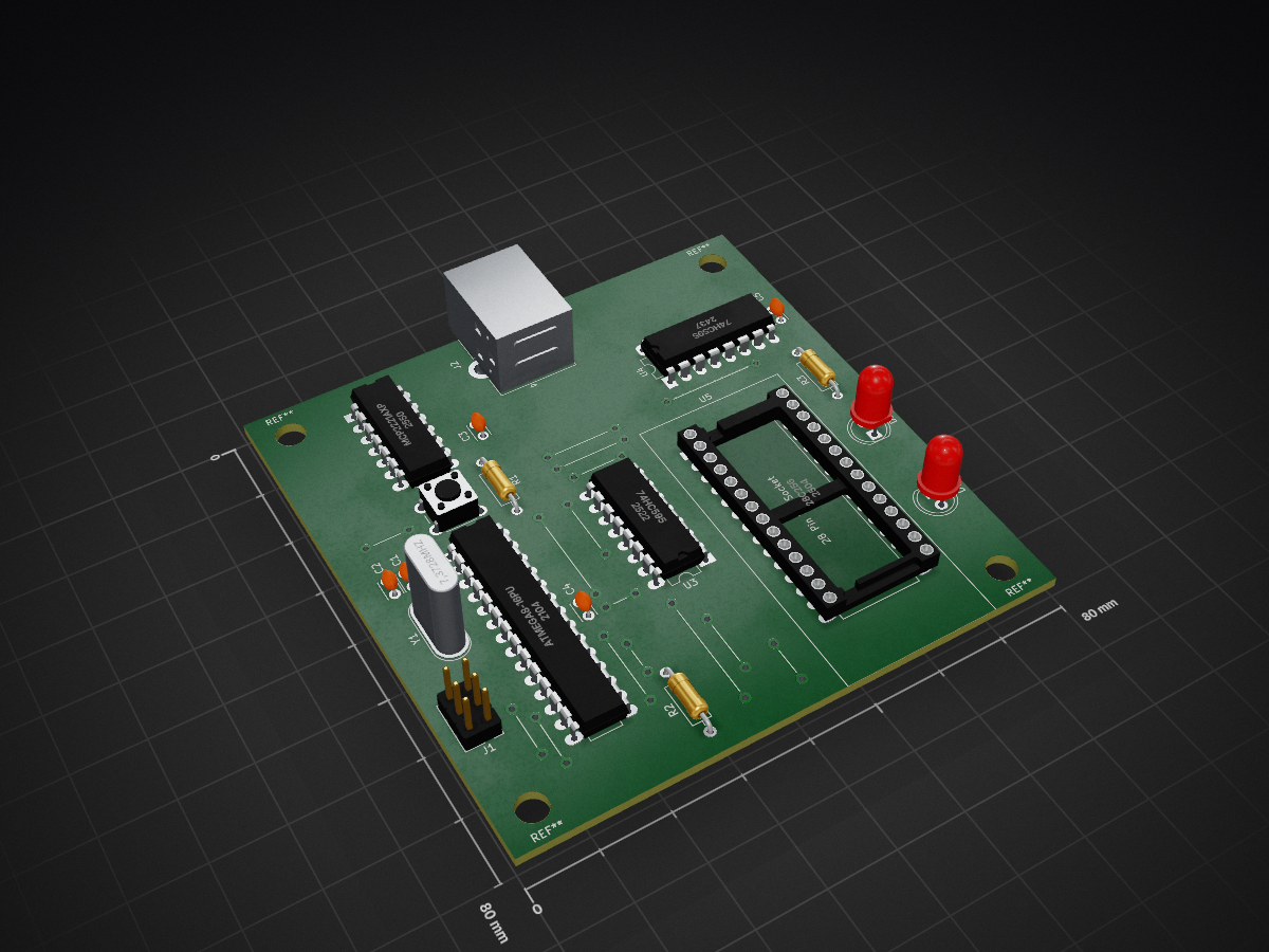
Eeprom programmer is an open-source printed circuit board by jkreucher, from the jkreucher/eeprom-programmer repository on GitHub, published under the MIT licence. It is a 2-layer board of 80 × 80 mm with 23 parts on 55 nets, routed with 372 tracks and 30 vias.
It is built around the ATMEGA8-16PU and 74HC595. Its parts include 5 capacitors, 5 ICs, 3 resistors, 2 diodes and 2 connectors. It belongs with the interfaces and adapters and retro computing and games boards and the AVR (ATmega, ATtiny) boards of this library.


Copyright 2021 Jannik Kreucher
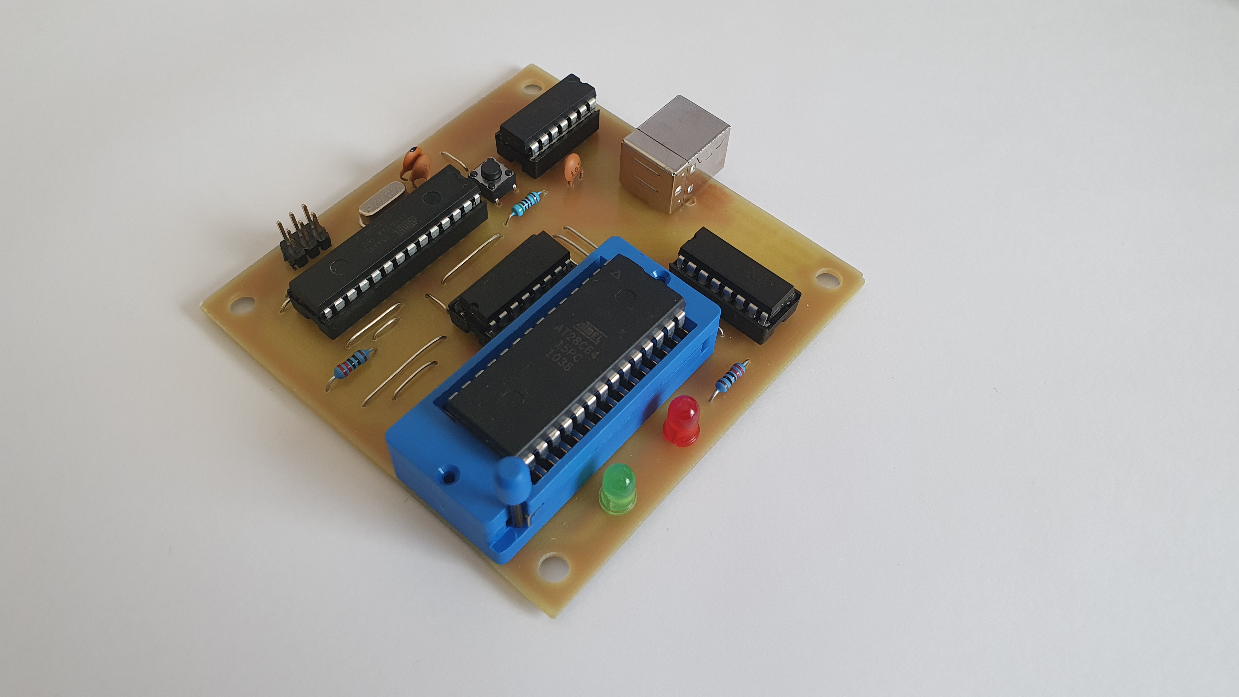
I created this programmer for my personal Z80 project. Since commerical programmers are fairly expensive I created my own simple programmer. It is nothing fancy and just supports a single family of EEPROMs. It does not have support for a higher programming voltage and is limited for +5V EEPROMs.
This simple programmer supports following EEPROMs:
To compile the code you need to have following tools installed:
The programmer flash tool uses Python3 and pySerial:
The Makefile contains a command to install everything needed:
cd code
sudo make toolsFirst compile the ATmega code. Execute following in the project root folder:
cd code
make
Now flash the compiled code to the programmer. Connect the ISP-Programmer and execute:
make fuses
make upload
I am using a USBasp Programmer. Note: Notch on ISP-Programmer must be facing the ATmega8 chip (U1) while flashing firmware.
Note: Firmware needs to be flashed beforehand !
To flash your binary file to the EEPROM inserted type:
cd code
chmod +x eeprom.py
./eeprom.py -e -o -p /dev/ttyACM0 -b 115200 -w <binaryfile.bin>
For more information:
./eeprom.py -h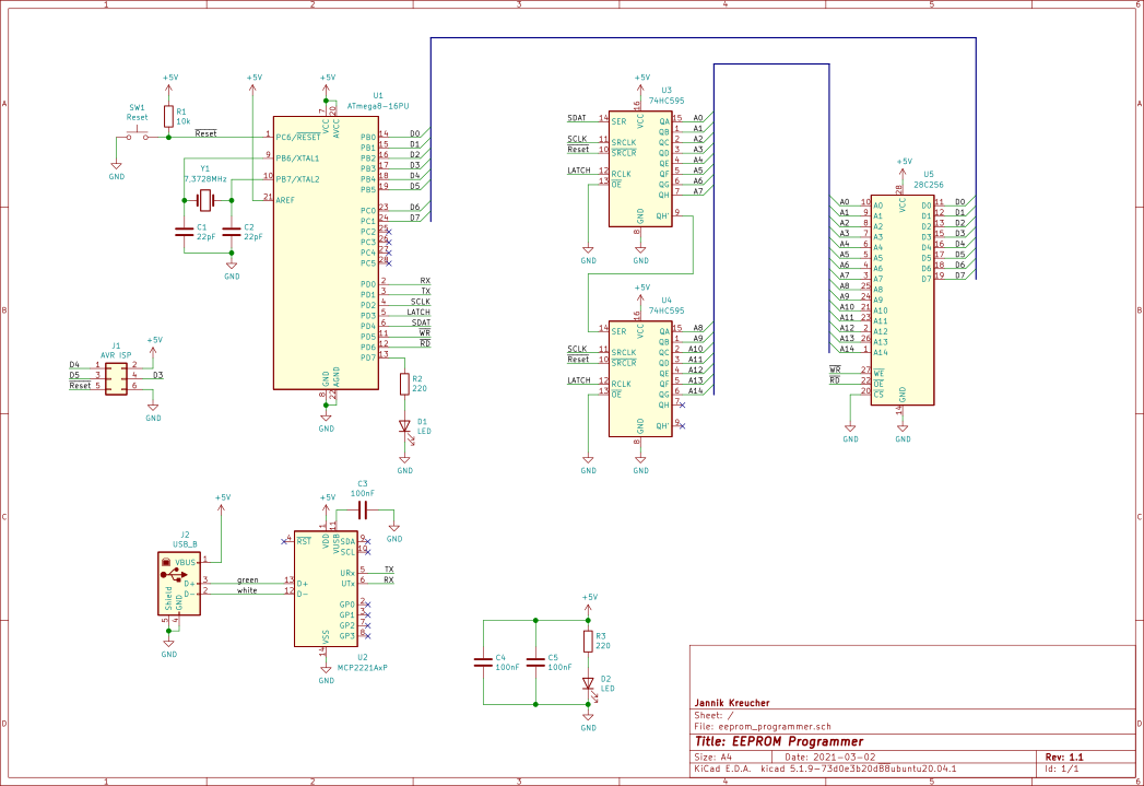
The micro processor used in this project is the popular ATmega8 (U1), a cheaper version of the ATmega328 used in the Arduino Uno. It handles everything: the serial communication, address bus and the data bus. U2 (MCP2221) handles the USB to UART conversion so no external ftdi cable is needed. The supply voltage is conveniantly given by the USB port also. Because data bus of the EEPROM is bidirectional it is directly connected to the processor. The micro processor needs to handle setting the bus as input or output. See eeprom.c for everything I/O related. The UART is handled in uart.c. And the communication protocol is defined in parser.c and in main.c.
The shift registers (U3, U4) are utilized to expand the IO of the processor. Just 3 bits are needed to set the address bus to the target address. Since the address bus is only one way no data needs to be read from the address bus thus making shift registers the obvious choice for this situation. See eeprom.c: addrbus_set() for how the data is latched.
The EEPROM uses a parallel interface for communication. The address bus (A0-A14) is a parallel input which sets the memory location to read or write. The control lines ~WE and ~OE (active low) tell the EEPROM to read or write from/to the memory. The data is read from or sent out the parallel data bus (D0-D7) depending on the state of the control lines. Some EEPROMs have Write-Protect enabled. A algorithm (see datasheet) is implemented to deactivate write protection. See eeprom.c: eeprom_disable_protect() for how this works.
Note: The pcb is designed so that the top layer represents jumpers. The vias are large enough to stick a wire through.
For the schematic and pcb layout I used KiCad, a very awsome open source EDA. The clearances and spaces are designed for diy home etching so nothing really fancy. See eeprom_programmer_bom.pdf for the bill of materials. At the moment the whole project would cost you around 26€ plus a weekend of time.
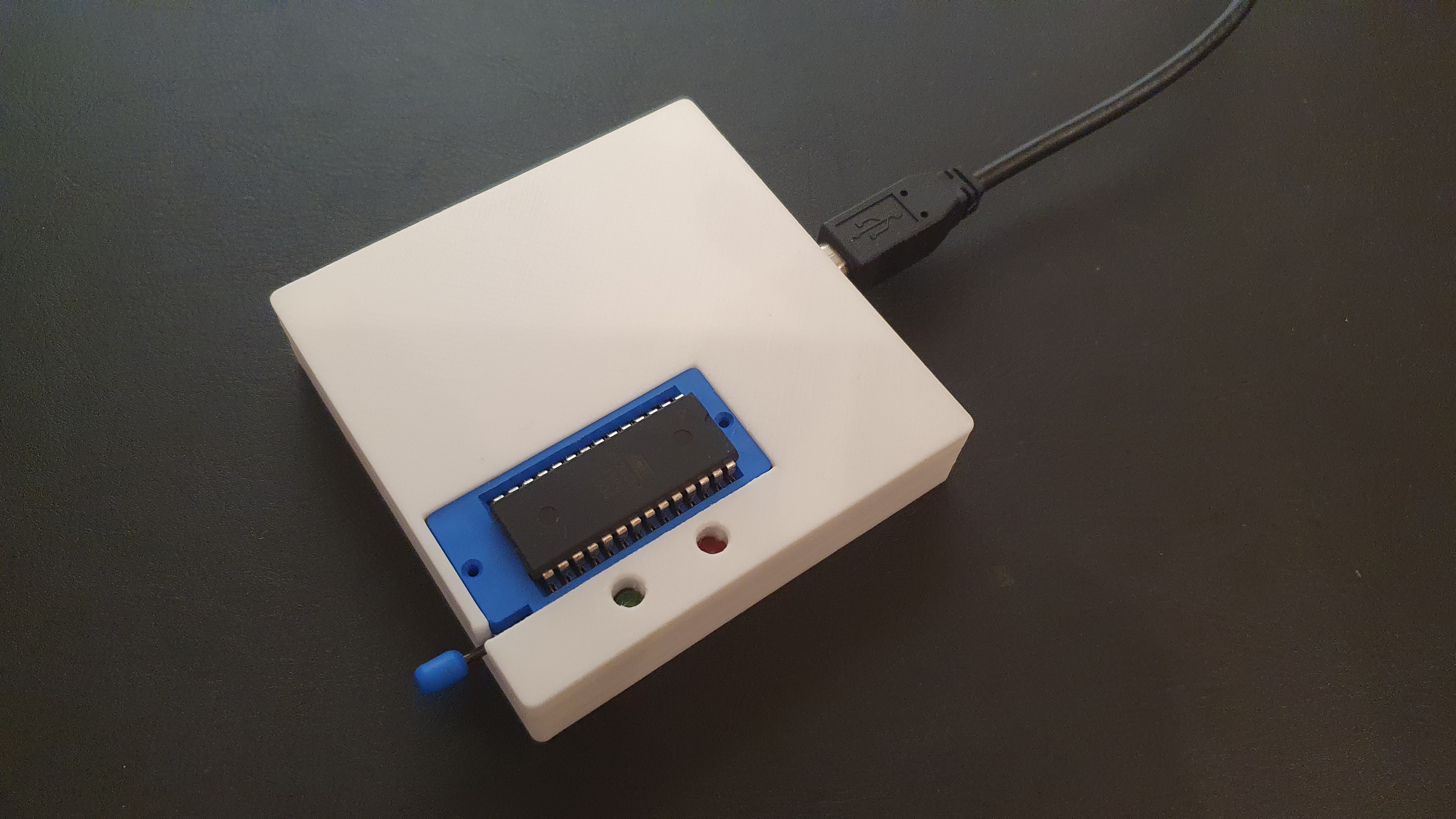
The very simple, easy and fast to print enclosure consists of two parts which sandwhich the pcb. Needed are just 4x M3,5x12mm wood screws to assemble the enclosure.
MIT Jannik Kreucher
| Qty | Value | Footprint | References |
|---|---|---|---|
| 3 | 100nF | Capacitor_THT:C_Disc_D3.0mm_W2.0mm_P2.50mm | C3, C4, C5 |
| 2 | 220 | Resistor_THT:R_Axial_DIN0207_L6.3mm_D2.5mm_P10.16mm_Horizontal | R2, R3 |
| 2 | 22pF | Capacitor_THT:C_Disc_D3.0mm_W2.0mm_P2.50mm | C1, C2 |
| 2 | 74HC595 | Package_DIP:DIP-16_W7.62mm_LongPads | U3, U4 |
| 2 | LED | LED_THT:LED_D5.0mm | D1, D2 |
| 1 | 10k | Resistor_THT:R_Axial_DIN0207_L6.3mm_D2.5mm_P10.16mm_Horizontal | R1 |
| 1 | 28C256 | zif:DIP-28_W15.24mm_ZIF_LongPads | U5 |
| 1 | 7,3728MHz | Crystal:Crystal_HC49-U_Vertical | Y1 |
| 1 | ATmega8-16PU | Package_DIP:DIP-28_W7.62mm_LongPads | U1 |
| 1 | AVR ISP | Connector_PinHeader_2.54mm:PinHeader_2x03_P2.54mm_Vertical | J1 |
| 1 | MCP2221AxP | Package_DIP:DIP-14_W7.62mm_LongPads | U2 |
| 1 | Reset | Button_Switch_THT:SW_PUSH_6mm | SW1 |
| 1 | USB_B | Connector_USB:USB_B_Lumberg_2411_02_Horizontal | J2 |
The 19 most common of 23 parts.
It measures 80 × 80 mm and has 2 copper layers, 1.6 mm thick.
23 parts, built around the ATMEGA8-16PU and 74HC595. The full list of its parts is on this page, with links to each part's symbol and footprint where PCBKit's library has them.
From the jkreucher/eeprom-programmer repository on GitHub, at the commit this page was made from: the board is eeprom_programmer.kicad_pcb. PCBKit opens the board in the browser, with nothing to install.
Its repository publishes it under the MIT licence: you may reuse it on that licence's terms (keep the author's notice, and for a copyleft licence share your changes alike).


ThKattanek/lan64usb
Diese Hard- und Software ermöglicht den Transfer von Programmen vom PC zum Commodore 64 (C64).


ondras12345/vetrnik
Electronics for heating water with power from a 2 kW wind turbine


dineshannayya/riscduino_board
Riscduino PCB Board documentation