
2 layers33.7 × 97.8 mm
HAN ESP TSS721
UtilitechAS/amsreader-firmware
ESP8266 and ESP32 compatible firmware to read, interpret and publish data to MQTT from smart electrical meters, both DLMS and DSMR is supported
29 parts470

 jijiaceness/custom-keyboard
Construction of a custom split keyboard for Keeb YSWS project
Left keyboard is an open-source printed circuit board by jijiaceness, from the jijiaceness/custom-keyboard repository on GitHub. It is a 2-layer board of 169.2 × 120.2 mm with 63 parts on 89 nets, routed with 310 tracks and 7 vias.
It is built around the RJ45. Its parts include 28 diodes, 28 switches, 1 IC and 1 connector. It belongs with the keyboards and input boards and the RP2040 boards of this library.
This is a fully custom 55-key split mechanical keyboard built from scratch, from the PCB to the 3D-printed case, developed with the support of Hack Club Program Keeb. I came into this project with almost no knowledge of how a keyboard works or the parts it consisted of, and over this two-month journey, I learned how to make all the components that make up a functional keyboard.
I've been wanting a split keyboard for a while after typing for hours on my laptop and experiencing hand pain and cramps. Mechanical keyboards have always appealed to me, and the Hack Club program Keeb was a great opportunity for me to build my own while learning the inner workings of a keyboard. I also liked the idea of how customizable my own keyboard would be as I could code what each key does instead of relying on the built-in funcitonality.
Again, I came into this endeavor with no idea what a switch even was, so I most likely learned more from building this keyboard than in any of my year-long classes at school.
I learned ...
The biggest challenge was definitely getting used to the applications (KiCad and Onshape) and their workflow. Not understanding the right sequence and way to do things, even with the help of Keeb's guide, cost me many hours of redoing things and searching into the depths of the internet to fix.
For KiCad, I didn't really finalize my layout on the schematic before moving onto the PCB editor and also put my left and right PCB on the same project, which went against KiCad's method of designing PCBs. I spent a lot of time moving the right PCB into a new project but still had to redo most of it.
For Onshape, I had no idea how to properly constrain my sketches, and my first iterations were filled with haphazard lengths and angles. I probably redid my sketch 10 times while designing the case. I do feel proud now in how far I've come in CADing since the beginning, and my sketches are much cleaner now.
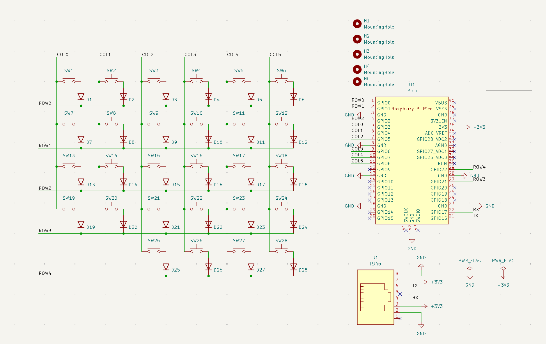
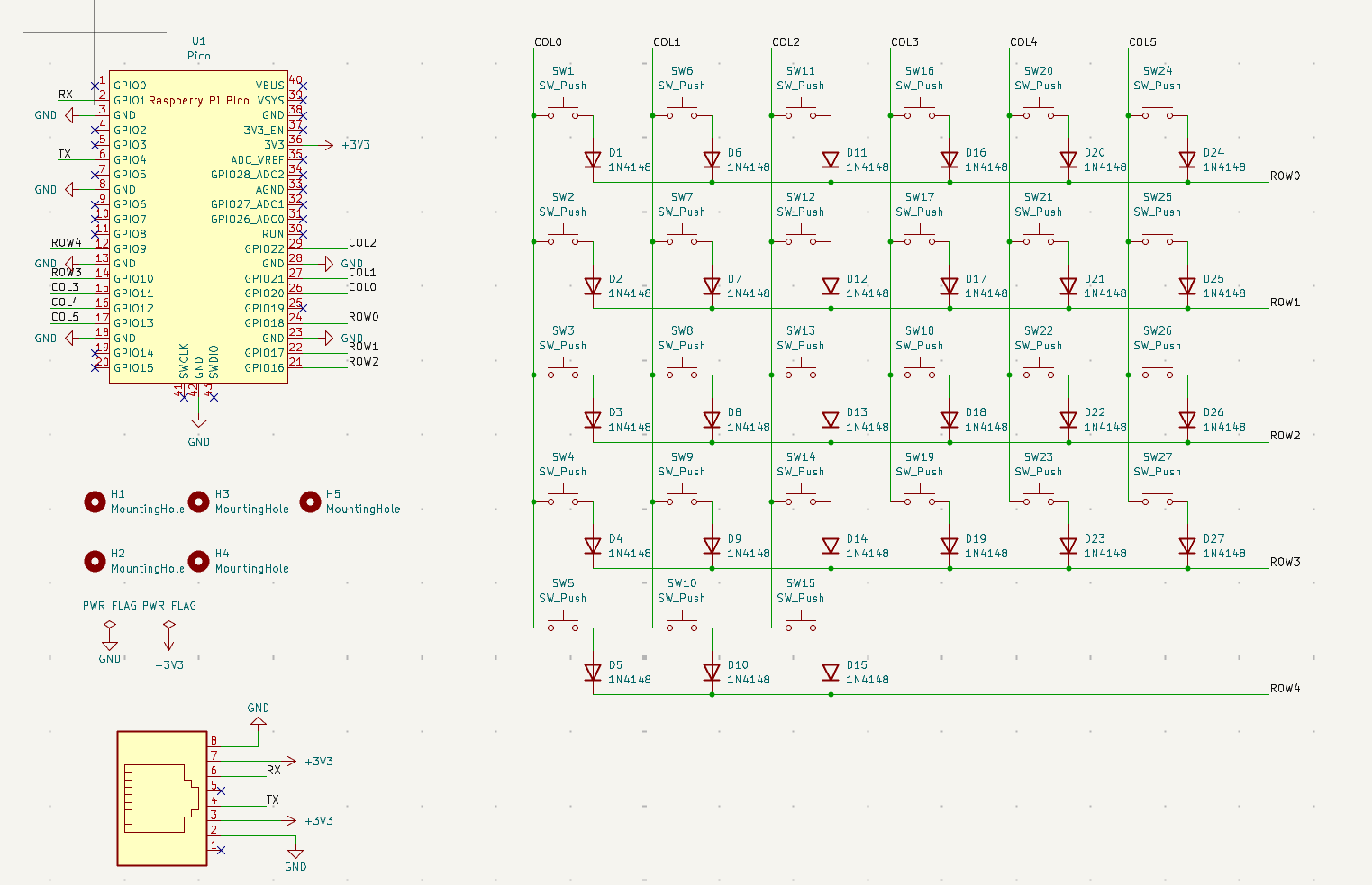
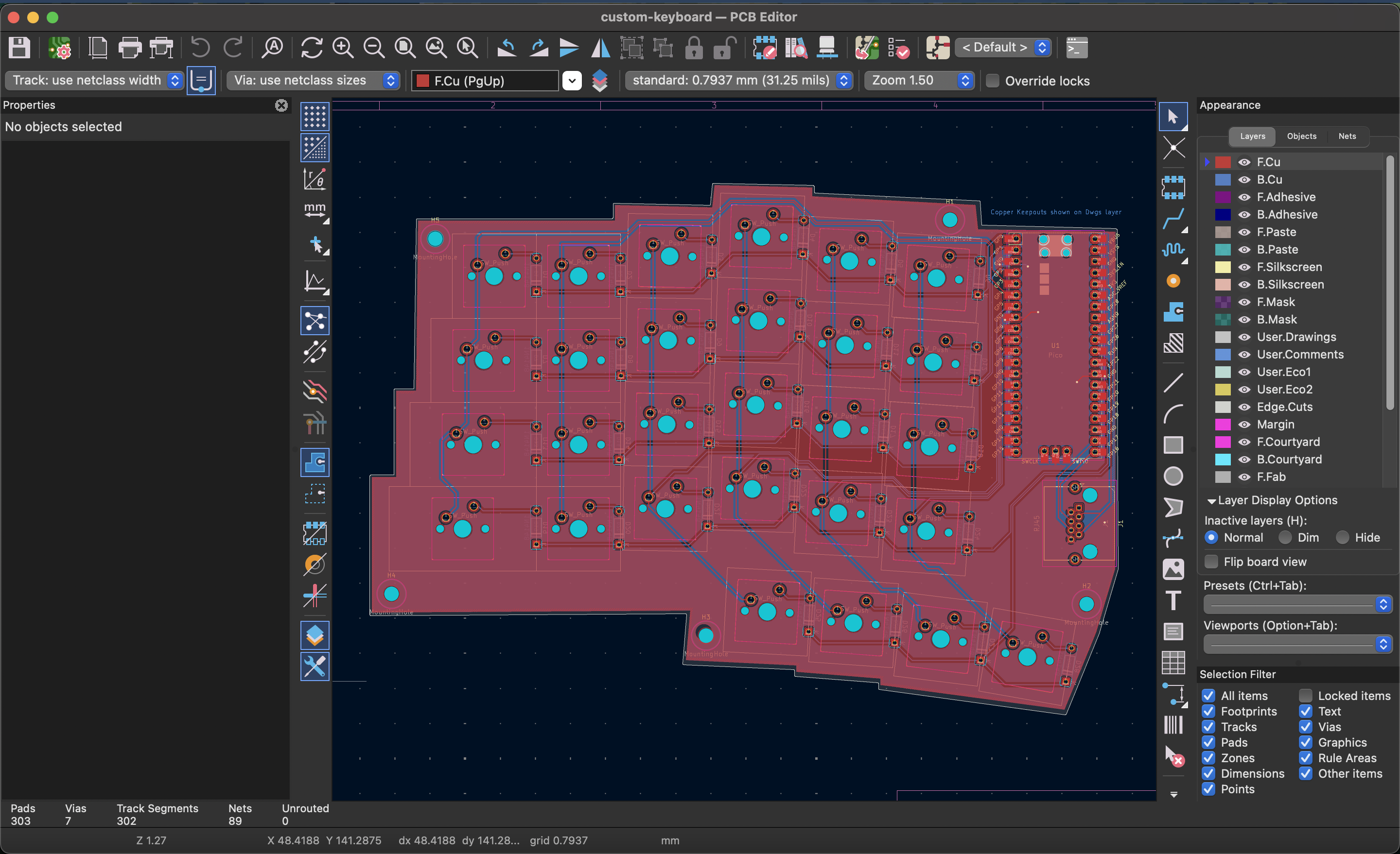
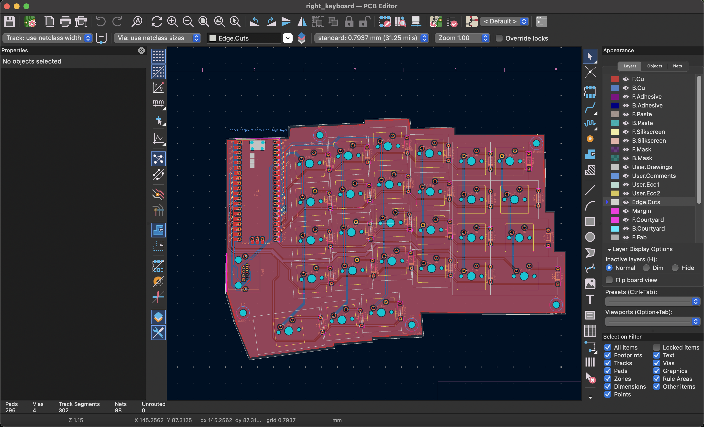
| left view | right view |
|---|---|
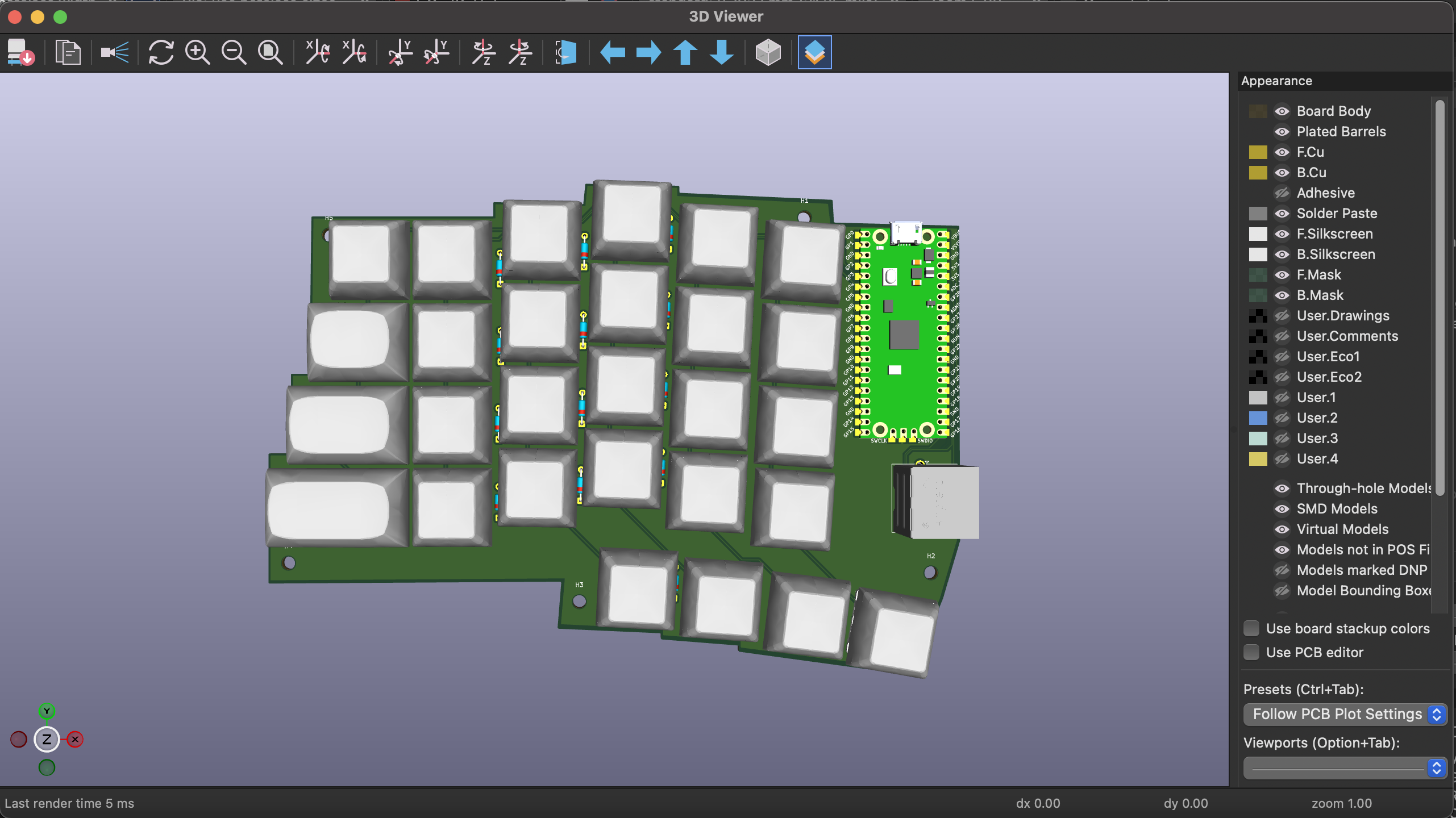 | 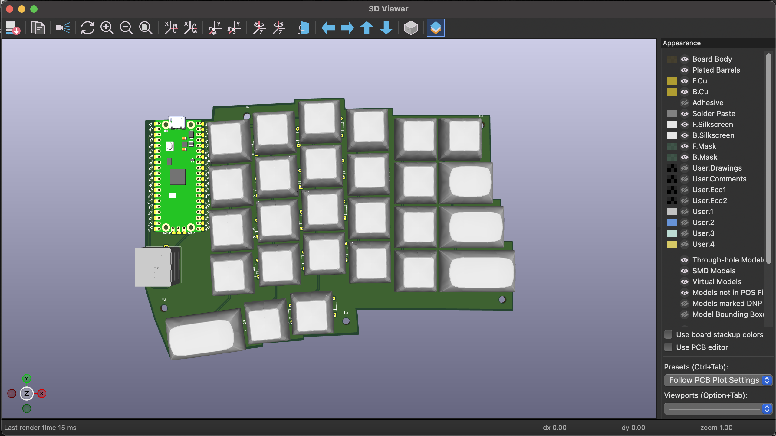 |
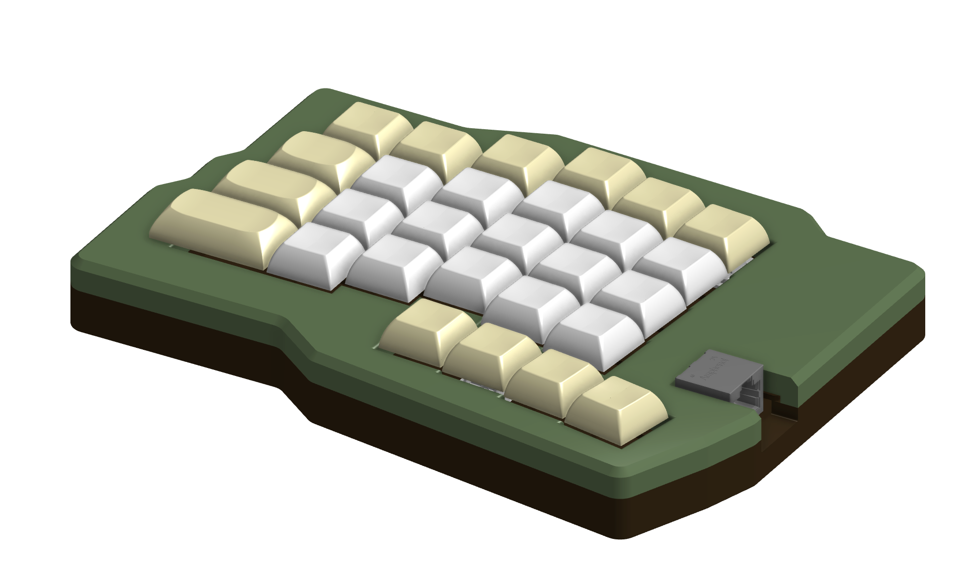
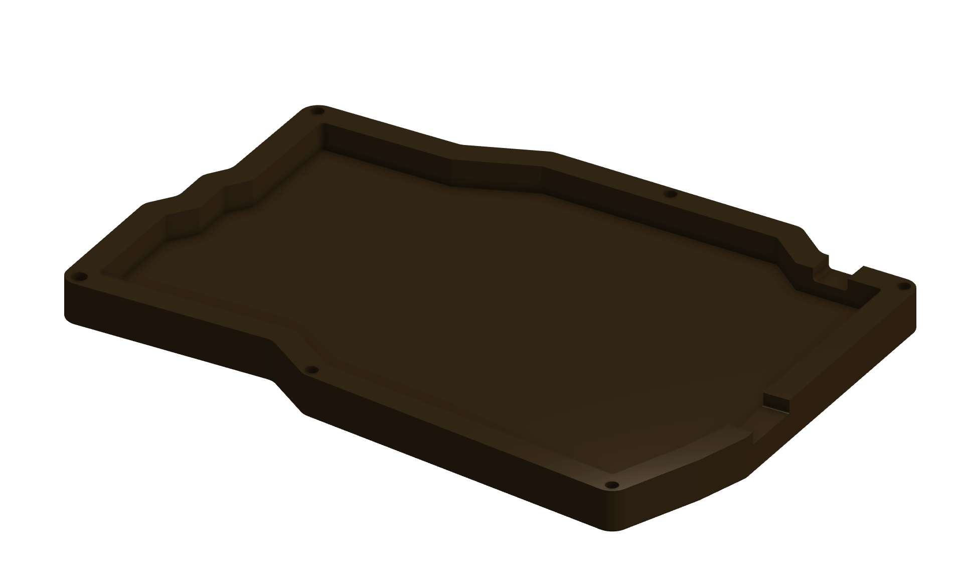
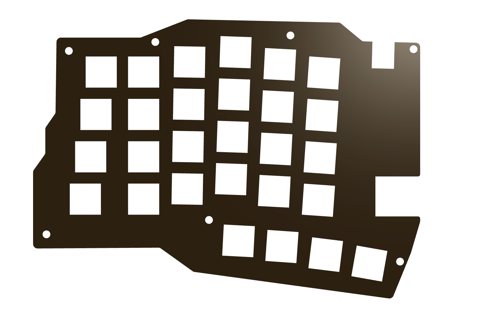
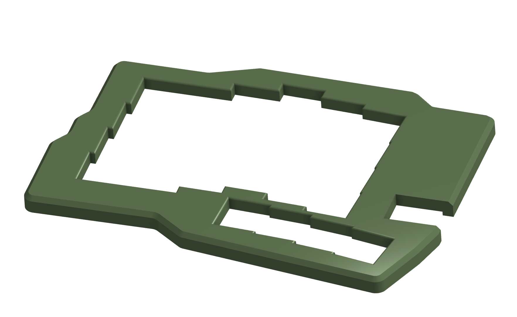
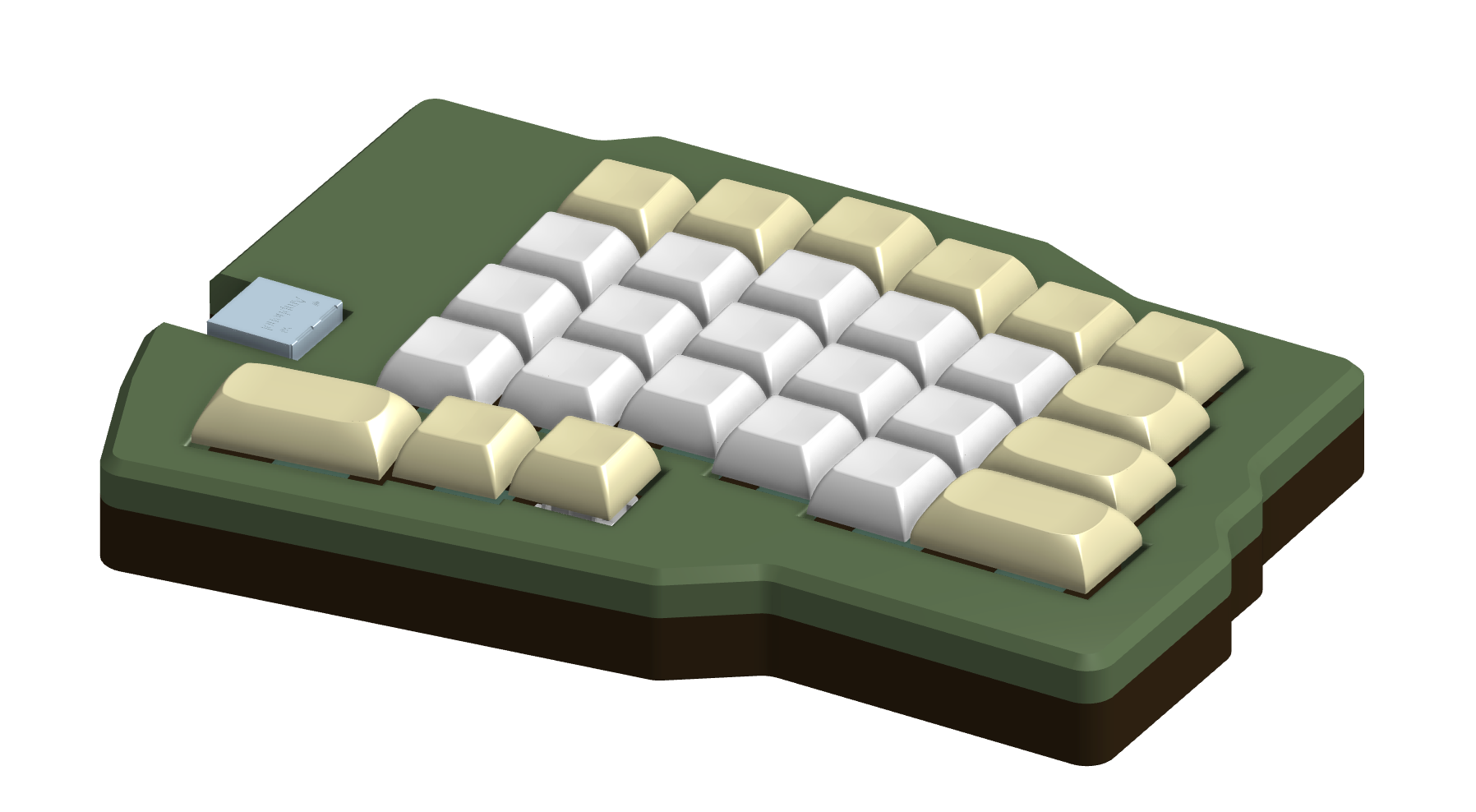
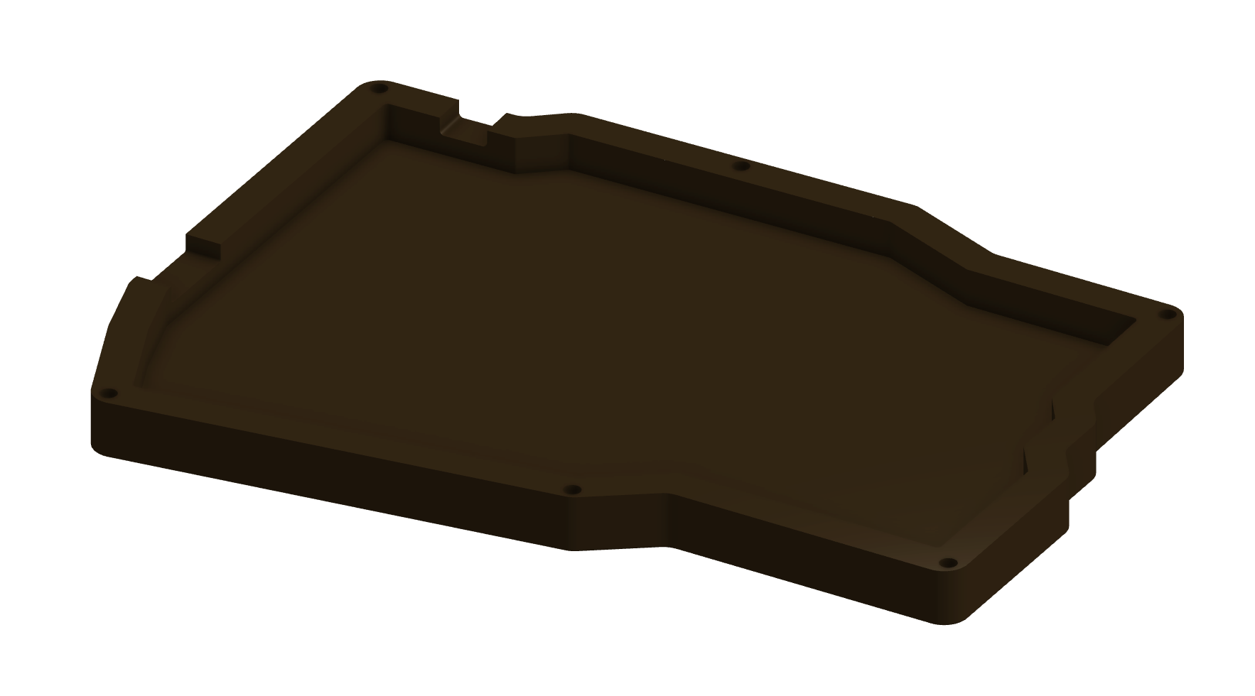
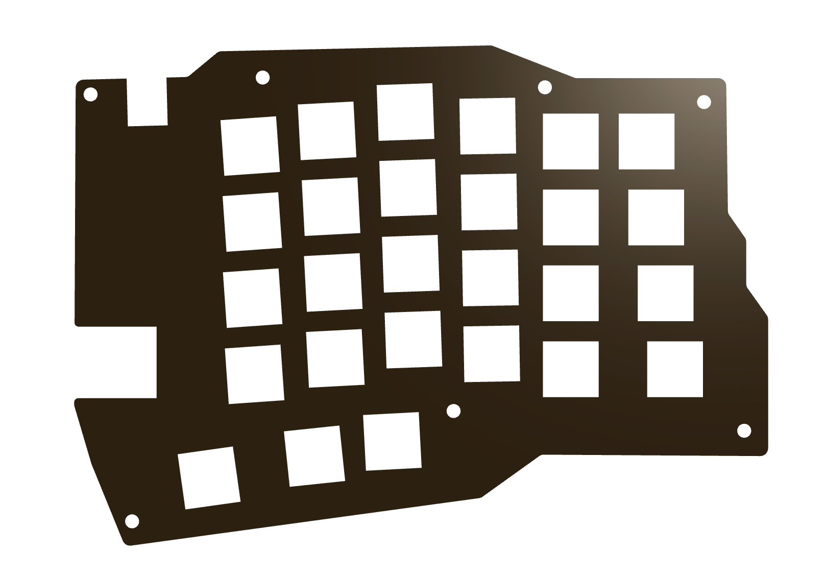
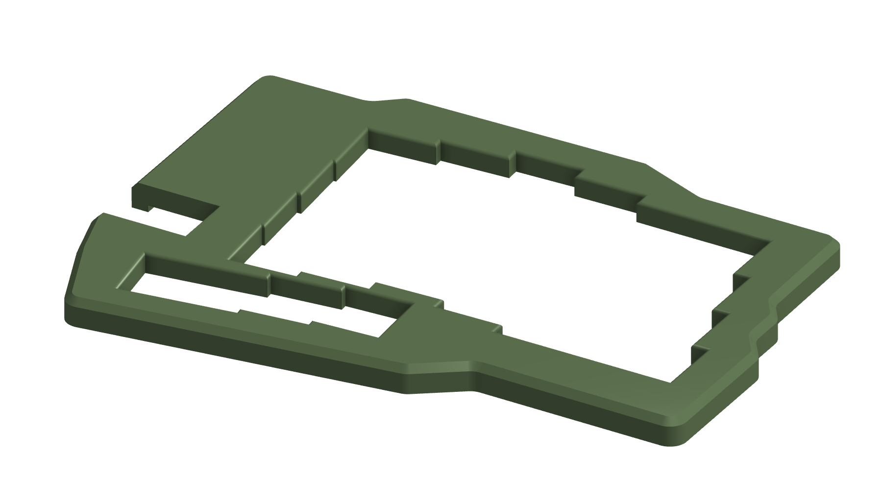
| Item | Name | Quantity | Notes | Cost (USD) |
|---|---|---|---|---|
| 1 | Raspberry Pi Pico | 2 | SC0916 | $7.82 |
| 2 | Left PCB from JLCPCB | 1 | $13.8 | |
| 3 | Right PCB from JLCPCB | 1 | $13.8 | |
| 4 | Cherry MX Switches | 55 | 70 count, Orange key switch. | $16.8 |
| 5 | 1N4148 Diodes | 55 | 100 count | $3.91 |
| 6 | M3xD4.6xL3.0 heatset inserts | 52 | 100 count | $5.18 |
| 7 | M3x5mm screws | 7 | 50 count | $2.56 |
| 8 | M3x14mm screws | 6 | 50 count | $3.54 |
| 9 | RJ45 Shield Network Jack | 2 | Comes in pack of 2, RJHSE-XM80 | $3.82 |
| 10 | Micro USB to USB-A Cable | 1 | 1m | $2.6 |
| 11 | USB-A to USB-C adapter | 1 | $3.45 | |
| 12 | Rj45 Connector | 1 | 0.5m | $4.37 |
| 13 | DSA Blank Custom Keycaps | 62 | 85 pcs (any keycaps bigger than 1u counts as 2 pcs | $32.94 |
| 14 | ||||
| TOTAL | $114.59 |
This project was possible due to the numerous open-source projects and resources, especially the the keyther by MagoSaronno as well as many other detailed in the journal. Finally, thank you to Hack Club Keeb for providing the guides and opportunity for me to build a keyboard!
| Qty | Value | Footprint | References |
|---|---|---|---|
| 28 | 1N4148 | Diode_THT:D_DO-35_SOD27_P7.62mm_Horizontal | D1, D2, D10, D11, D12, D13, D14, D15, D16, D17, D18, D19, D20, D21, D22, D23 +12 |
| 25 | SW_Push | PCM_marbastlib-mx:SW_MX_1u | SW1, SW2, SW10, SW11, SW12, SW14, SW15, SW16, SW17, SW18, SW20, SW21, SW22, SW23, SW24, SW25 +9 |
| 5 | MountingHole | MountingHole:MountingHole_3.2mm_M3 | H1, H2, H3, H4, H5 |
| 1 | Pico | Raspberry_Pi_Pico_and_Boards:RPi_Pico_SMD_TH | U1 |
| 1 | RJ45 | Connector_RJ:RJ45_Amphenol_RJHSE5380 | J1 |
| 1 | SW_Push | PCM_marbastlib-mx:SW_MX_1.75u | SW19 |
| 1 | SW_Push | PCM_marbastlib-mx:SW_MX_1.5u | SW13 |
| 1 | SW_Push | PCM_marbastlib-mx:SW_MX_1.25u | SW7 |
UtilitechAS/amsreader-firmware
ESP8266 and ESP32 compatible firmware to read, interpret and publish data to MQTT from smart electrical meters, both DLMS and DSMR is supported

travisgoodspeed/goodfet
An embedded bus adapter for various microcontrollers and radios.


nv1t/standing-desk-interceptor
I wanted to intercept the communication between my Flexispot standing desk buttons. This is the progress on the project


Severson-Group/AMDC-Hardware
Circuit board designs for controlling advanced motor systems

mfkiwl/KiwiSDR_PCB
KiCAD PCB files for KiwiSDR project including active antenna and bias tee
It measures 169.2 × 120.2 mm and has 2 copper layers, 1.6 mm thick.
63 parts, built around the RJ45. The full list of its parts is on this page, with links to each part's symbol and footprint where PCBKit's library has them.
From the jijiaceness/custom-keyboard repository on GitHub, at the commit this page was made from: the board is pcb/left-keyboard.kicad_pcb and its schematic pcb/left-keyboard.kicad_sch. PCBKit opens the board in the browser, with nothing to install.
Its repository states no licence, so its author keeps all rights: ask jijiaceness before reusing the design.