
2 layers98.5 × 99.1 mm

 jgarr0/SDP-PCBs
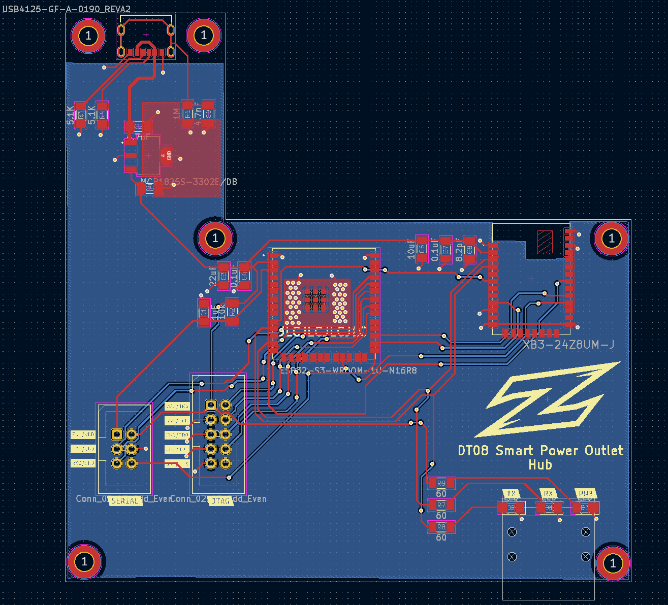
Outlet schematic is an open-source printed circuit board by jgarr0, from the jgarr0/SDP-PCBs repository on GitHub. It is a 2-layer board of 81.7 × 62.5 mm with 51 parts on 60 nets, routed with 632 tracks and 148 vias.
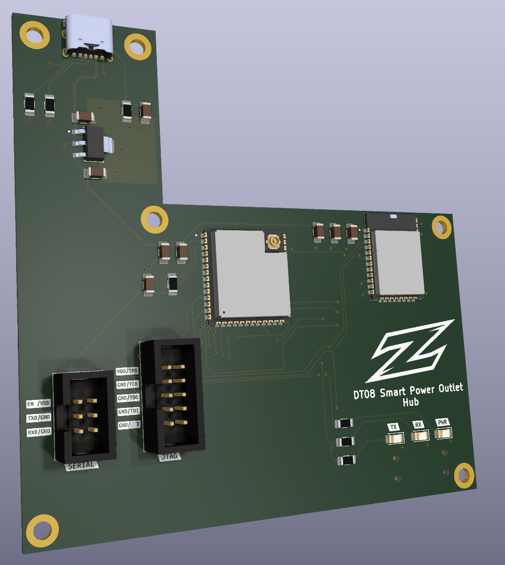
It is built around the ESP32-S3-WROOM-1U-N16R8 and XB3-24Z8UM-J. Its parts include 6 capacitors, 5 resistors, 4 diodes, 4 connectors and 2 ICs. It belongs with the ESP32 boards of this library.
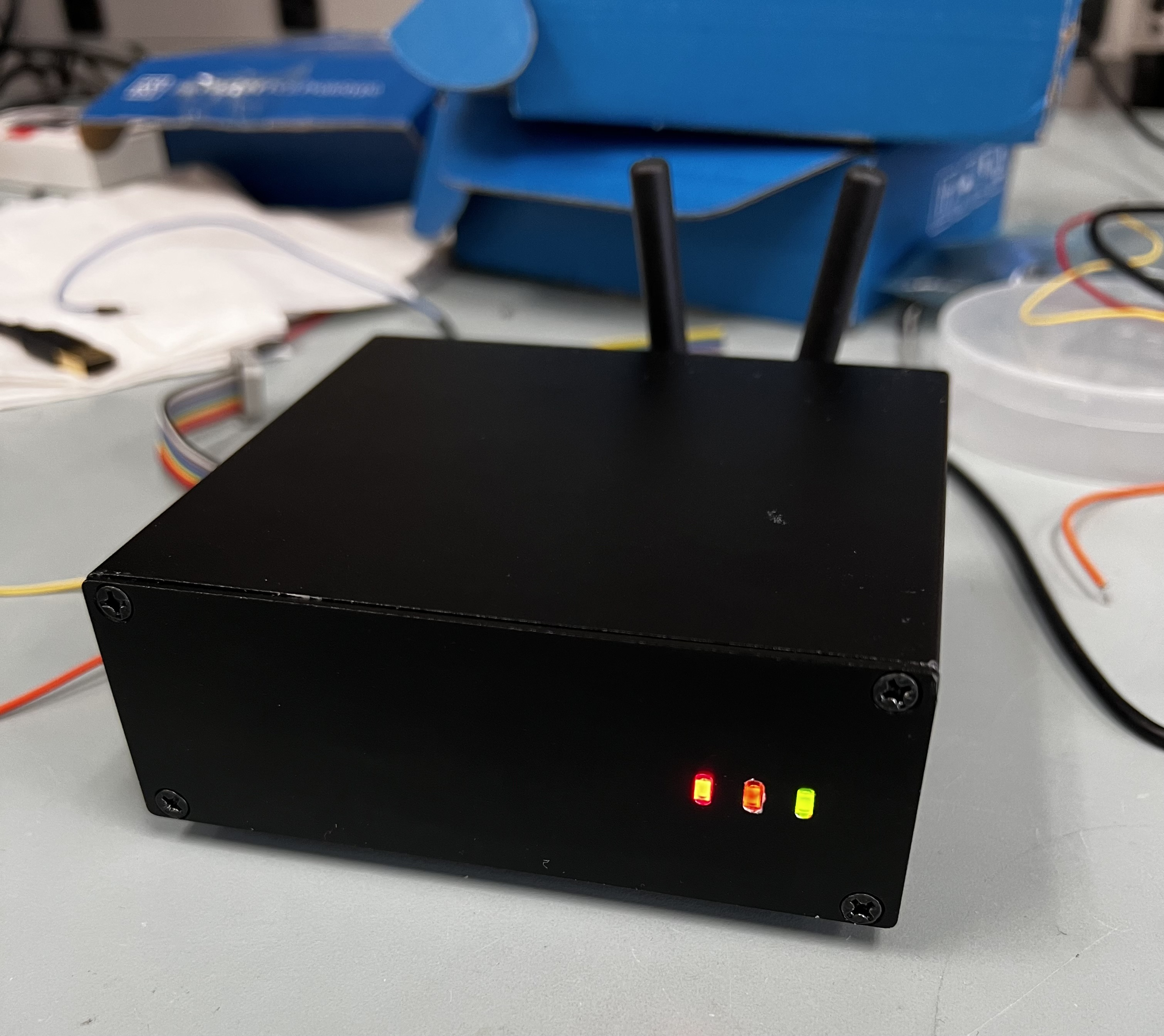
Hub and Outlet Motherboard Schematics and PCB Layouts for Smart Power Outlet System
#Hub PCB Schematic
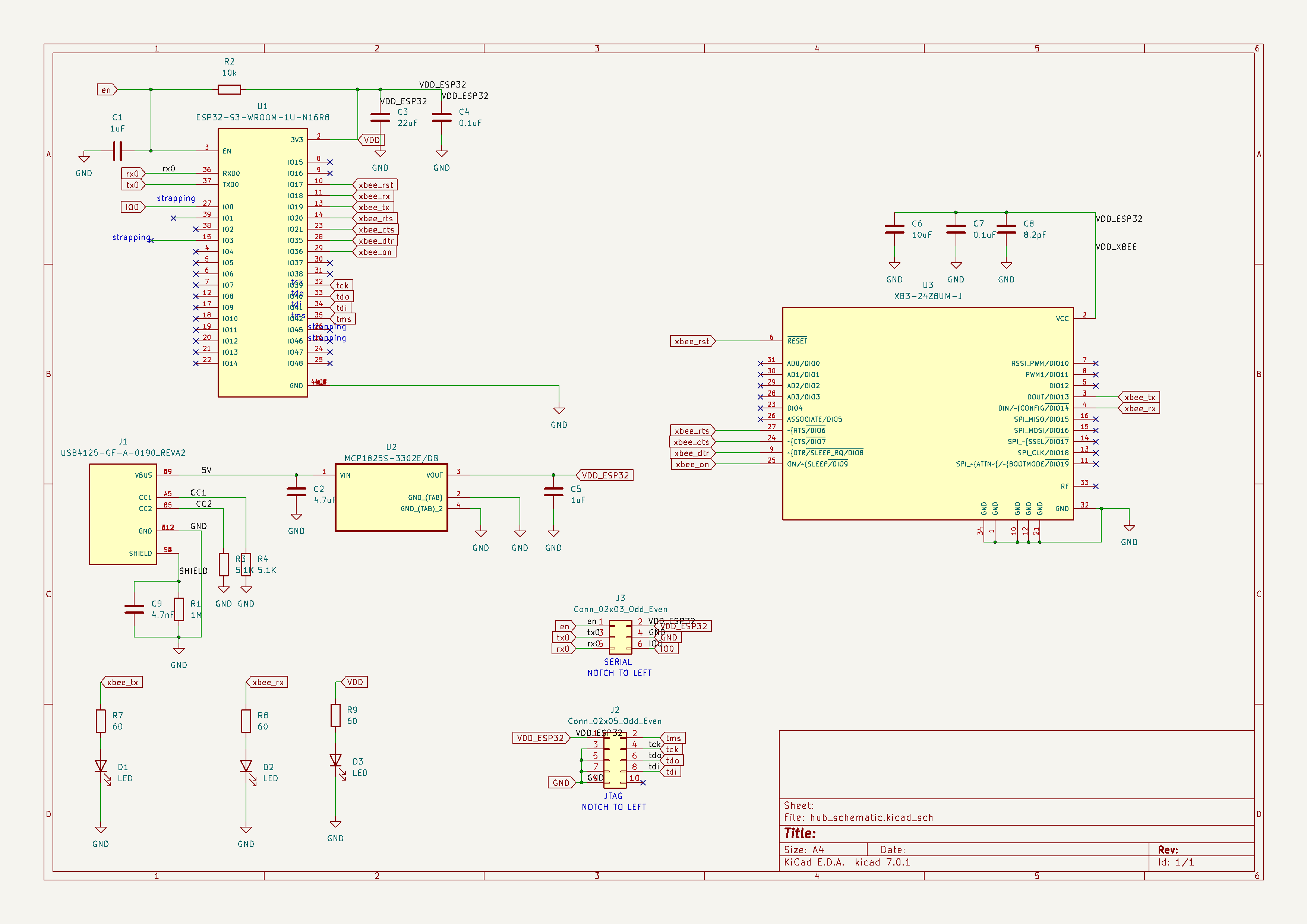
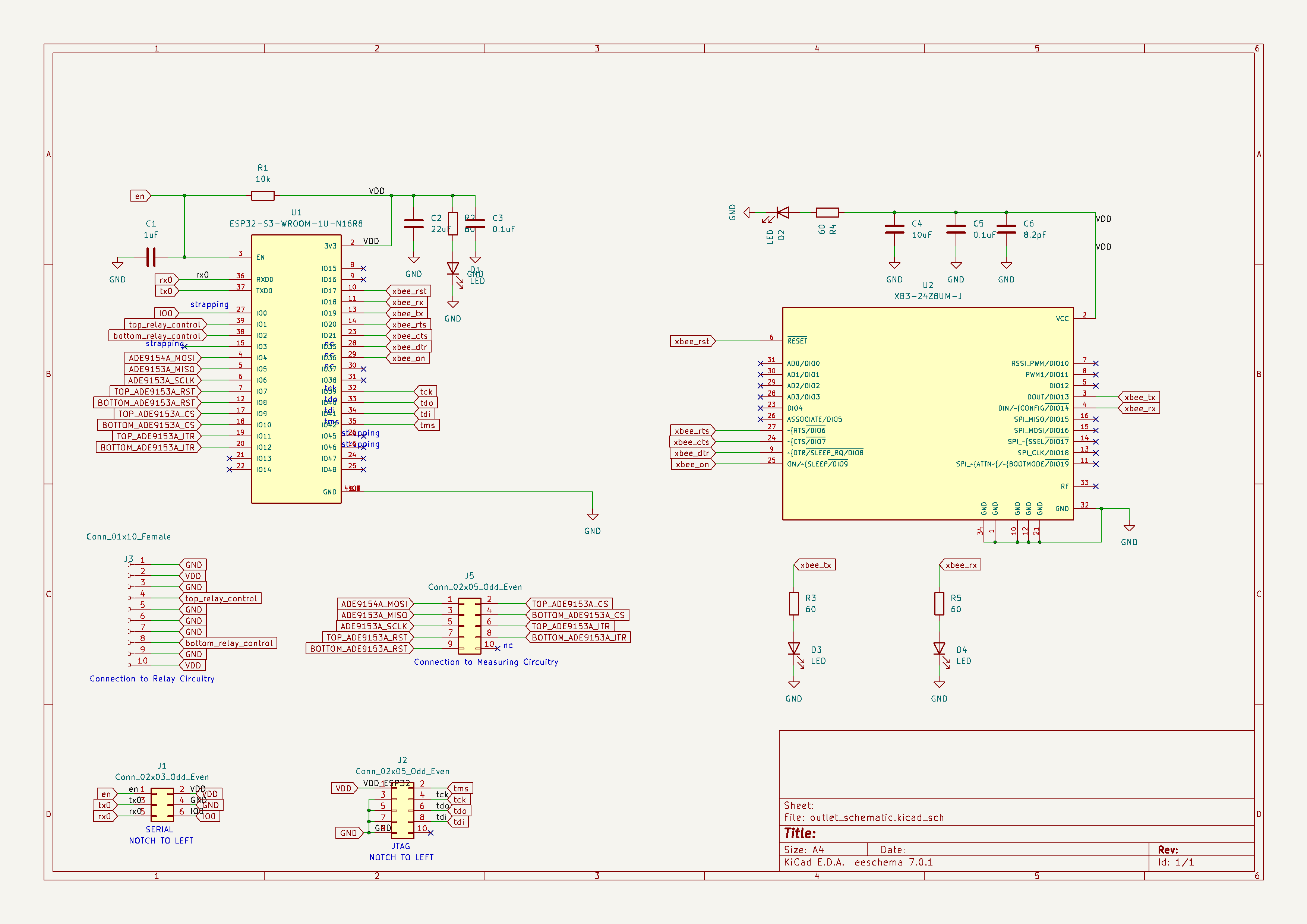
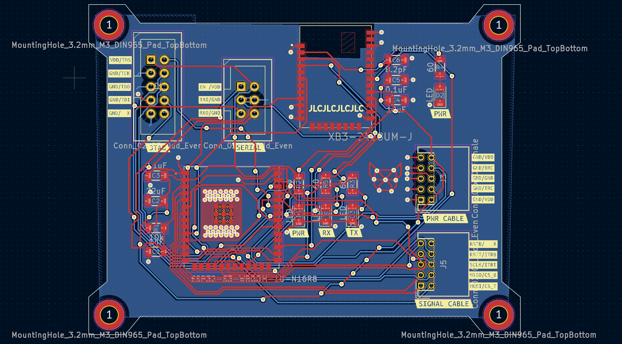
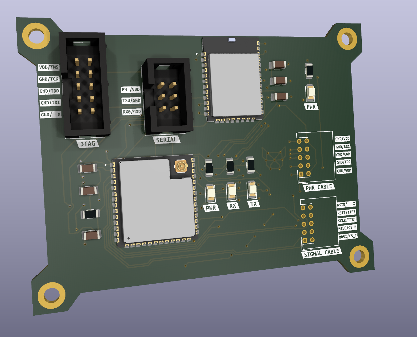
| Qty | Value | Footprint | References |
|---|---|---|---|
| 4 | 60 | Resistor_SMD:R_1206_3216Metric | R2, R3, R4, R5 |
| 4 | LED | LED_SMD:LED_1206_3216Metric | D1, D2, D3, D4 |
| 4 | MountingHole_3.2mm_M3_DIN965_Pad_TopBottom | MountingHole:MountingHole_3.2mm_M3_DIN965_Pad_TopBottom | MP1, MP2, MP3, MP4 |
| 2 | 0.1uF | Capacitor_SMD:C_1206_3216Metric | C3, C5 |
| 2 | G*** | kibuzzard-64222CB8 | kibuzzard-64222CB8, kibuzzard-64222CB8 |
| 1 | 10k | Resistor_SMD:R_1206_3216Metric | R1 |
| 1 | 10uF | Capacitor_SMD:C_1206_3216Metric | C4 |
| 1 | 1uF | Capacitor_SMD:C_1206_3216Metric | C1 |
| 1 | 22uF | Capacitor_SMD:C_1206_3216Metric | C2 |
| 1 | 8.2pF | Capacitor_SMD:C_1206_3216Metric | C6 |
| 1 | Conn_01x10_Female | Connector_JST:JST_PHD_S10B-PHDSS_2x05_P2.00mm_Horizontal | J3 |
| 1 | Conn_02x03_Odd_Even | Connector_IDC:IDC-Header_2x03_P2.54mm_Vertical | J1 |
| 1 | Conn_02x05_Odd_Even | Connector_IDC:IDC-Header_2x05_P2.54mm_Vertical | J2 |
| 1 | Conn_02x05_Odd_Even | Connector_JST:JST_PHD_S10B-PHDSS_2x05_P2.00mm_Horizontal | J5 |
| 1 | ESP32-S3-WROOM-1U-N16R8 | SnapEDA Library:XCVR_ESP32-S3-WROOM-1U | U1 |
| 1 | G*** | kibuzzard-64222F0B | kibuzzard-64222F0B |
| 1 | G*** | kibuzzard-64223346 | kibuzzard-64223346 |
| 1 | G*** | kibuzzard-6423A409 | kibuzzard-6423A409 |
| 1 | G*** | kibuzzard-64223022 | kibuzzard-64223022 |
| 1 | G*** | kibuzzard-64222ED4 | kibuzzard-64222ED4 |
| 1 | G*** | kibuzzard-64223357 | kibuzzard-64223357 |
| 1 | G*** | kibuzzard-6422317A | kibuzzard-6422317A |
| 1 | G*** | kibuzzard-64223322 | kibuzzard-64223322 |
| 1 | G*** | kibuzzard-6422333F | kibuzzard-6422333F |
| 1 | G*** | kibuzzard-64223170 | kibuzzard-64223170 |
| 1 | G*** | kibuzzard-64222DA8 | kibuzzard-64222DA8 |
| 1 | G*** | kibuzzard-64222D21 | kibuzzard-64222D21 |
| 1 | G*** | kibuzzard-6422332A | kibuzzard-6422332A |
| 1 | G*** | kibuzzard-64223074 | kibuzzard-64223074 |
| 1 | G*** | kibuzzard-64223167 | kibuzzard-64223167 |
| 1 | G*** | kibuzzard-64222D10 | kibuzzard-64222D10 |
| 1 | G*** | kibuzzard-6422303A | kibuzzard-6422303A |
| 1 | G*** | kibuzzard-64222F16 | kibuzzard-64222F16 |
| 1 | G*** | kibuzzard-64222DBC | kibuzzard-64222DBC |
| 1 | G*** | kibuzzard-6422318F | kibuzzard-6422318F |
| 1 | G*** | kibuzzard-64223004 | kibuzzard-64223004 |
| 1 | G*** | kibuzzard-64222E4F | kibuzzard-64222E4F |
| 1 | G*** | kibuzzard-64223187 | kibuzzard-64223187 |
| 1 | G*** | kibuzzard-64222F2D | kibuzzard-64222F2D |
| 1 | XB3-24Z8UM-J | SnapEDA Library:XCVR_XB3-24Z8UM-J | U2 |

northernpaws/lasernet-rev1
Retrofit Zigbee PCBs, firmware, and a custom Linux-based game controller for the lasertag.net Falcon system.

mx3353672833-debug/moto-gps-waveshare
MOTO GPS · Waveshare ESP32-S3 1.75C 圆屏导航 + iPhone App | Author: Maler X | Noncommercial, attribution required | Experimental

portapack-mayhem/mayhem-mdk
PortaPack - Module Develoment Kit


m-kozlowski/airbridge
Wireless adapter for AirSense/AirCurve 10 devices


It measures 81.7 × 62.5 mm and has 2 copper layers, 1.6 mm thick.
51 parts, built around the ESP32-S3-WROOM-1U-N16R8 and XB3-24Z8UM-J. The full list of its parts is on this page, with links to each part's symbol and footprint where PCBKit's library has them.
From the jgarr0/SDP-PCBs repository on GitHub, at the commit this page was made from: the board is Outlet/outlet_schematic.kicad_pcb and its schematic Outlet/outlet_schematic.kicad_sch. PCBKit opens the board in the browser, with nothing to install.
Its repository states no licence, so its author keeps all rights: ask jgarr0 before reusing the design.