4 layers134 × 84.7 mm
 jeevan9s/homectrl-sys2
home automation controller
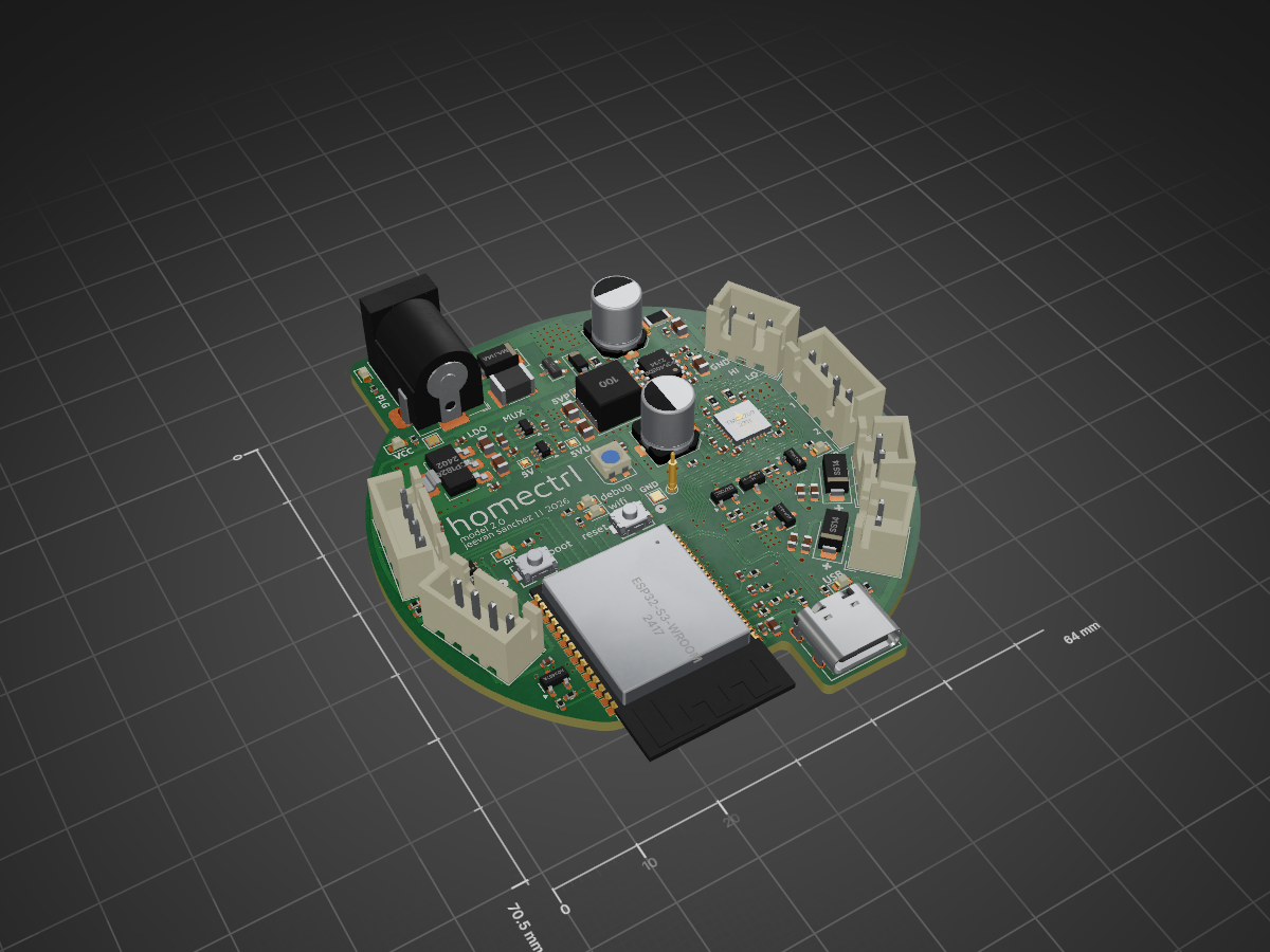
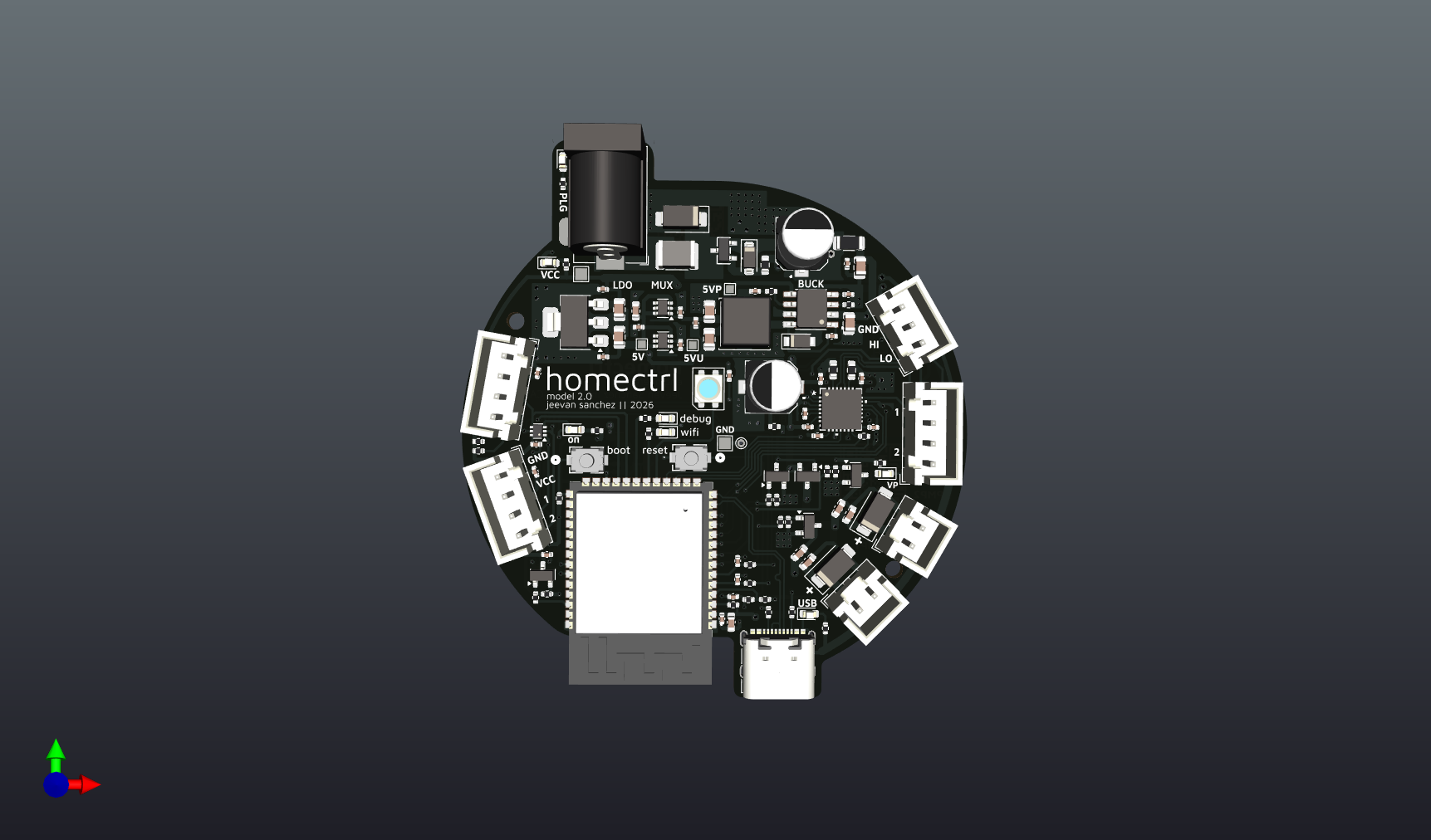
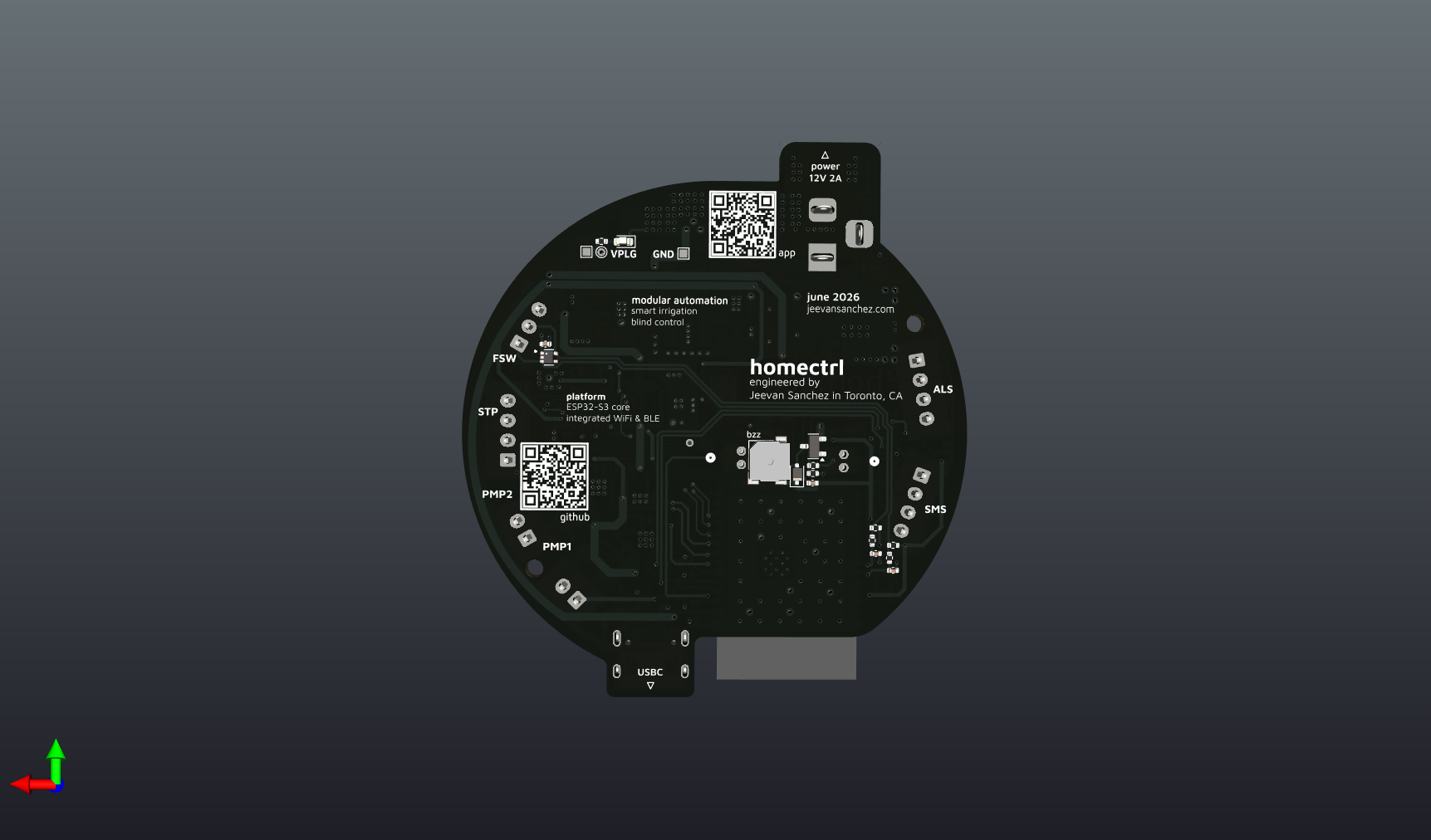
Homectrl v2 is an open-source printed circuit board by jeevan9s, from the jeevan9s/homectrl-sys repository on GitHub. It is a 4-layer board of 63.2 × 70.5 mm with 141 parts on 97 nets, routed with 953 tracks and 310 vias.
It is built around the ESP32-S3-WROOM-1-N8, DMP4065S-7 and SI2347DS-T1-GE3-1, with the TMC2209, TPD2E001DRLR and TPD4E001DRLR among its other parts. Its parts include 43 capacitors, 39 resistors, 15 diodes, 8 ICs and 8 connectors. It belongs with the radio and wireless and home automation and IoT boards and the ESP32 boards of this library.


Home-automation controller with a Next.js dashboard.
- Controller PCB currently being manufactures
- Firmware and docs development in progress.
- Mechanical components currently being printed.
I built homectrl because I wanted to automate my first apartment.
|
|
Practicality is a consistent motive when building.
As I moved into my first apartment during my first year at Queen's University, I wanted a device capable of smart-control for plants and window blinds, which are main components of my studio. This pushed me to build homectrl, a controller that leverages sensor readings, actuators, and WiFi for home automation.
The first version was manufactured in October of 2025, and this was my first PCB designed. It was a bit elementary, lots of breakout boards soldered on, an MCU devkit, etc. Over the year I designed several other PCBs and learned a lot, which pushed me to produce a second version that I can use reliably for my 2nd year in Kingston.
It's now June and the controller is being manufactured while I write docs and firmware.
The controller is powered by a 12V 2A adapter and driven by an ESP32-S3.
Below is a list of features from power circuits to various peripherals.
The controller communicates to a Next.js webapp via Websockets and is also connected to Alexa via SinricPro for voice control, over WiFi/MQTT.
This section provides low-level explanations of the significant circuits of each "module" of the controller.
I encourage you to clone the repo or you use KiCanvas to look at the schematic and board files.
All electronics were designed with KiCad.
Power Entry
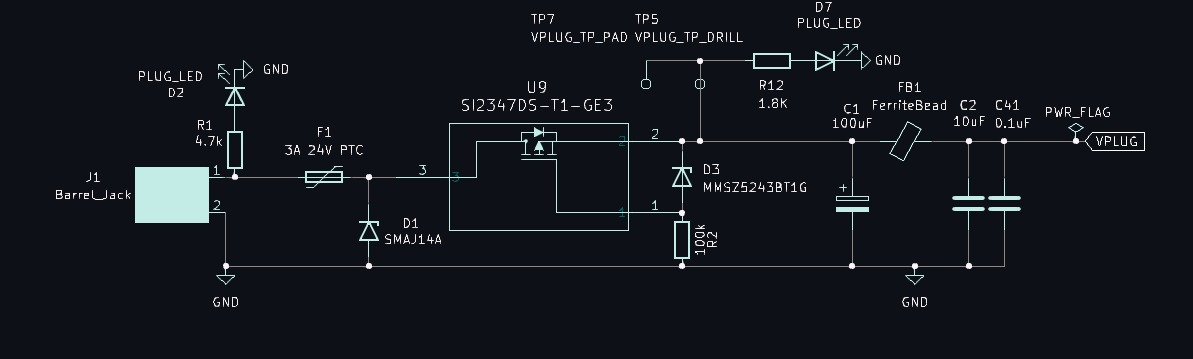
The 12V 2A power enters through a barrel jack connector, where it is then met with a 24V 3A fuse for over-current protection. A PTC resettable fuse was selected for durability.
The positive plug line VPLUG is then protected from voltage spikes with a Transient Voltage Supression (TVS) diode placed in paralell for clamping.
14V15.3V23.2VThe positive line then goes through a Reverse Polarity Protection (RPP) circuit, using a P-Channel MOSFET for lossless efficiency (lower V drop than standard diodes).
A Zener diode and resistor is placed between the MOSFET's gate and source for gate over-voltage protection.
A bulk electrolytic (100μF) capacitor, ferrite bead, and high-frequency (0.1μF) capacitor are then placed to create a third-order low pass filter (π-filter).
The ferrite bead was primariy selected for its saturation current and DCR.
The approximate current draw with safety margin $I_{net}$ is 2A.
$I_{\mathrm{sat}} = 1.5 \times I_{\mathrm{net}} \approx 3 A$
Minimize heat dissipation.
$DCR$ is 20Ω
$P_{heat} = DCR \times I_{\mathrm{sat}} \approx 0.06 W$
Voltage Regulation (I)
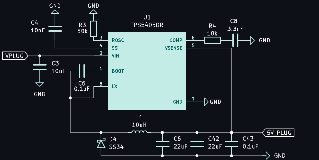
The controller uses a cascade regulation system, starting with the TPS5405DR buck converter.
The input voltage is VPLUG (12V), after the protection and filtering circuitry, and the output is 5V.
The $R_{osc}$ value will determine the switching frequency of the converter.
Switching frequency is governed by the relationship. $$R_{\text{OSC}} (\text{k}\Omega) = 21.82 \cdot f_{\text{SW}}^{-1.167}$$
I chose a value of 50kΩ for a $f_{SW}$ of approximately 525 kHz
For the soft-start capacitor $C_{ss}$ , I chose a value of 10nF for a soft-start time of 5ms
The values below were taken from the TPS5405DR Datasheet
$$ C_{SS} = \frac{t_{SS} \cdot I_{SS}}{V_{REF}} $$
$$ C_{SS} = \frac{(5,\mathrm{ms})(2,\mathrm{\mu A})}{0.8,\mathrm{V}} = 12.5,\mathrm{nF} \approx 10,\mathrm{nF} $$
The inductor values were chosen using the equation below.
$$ L=\frac{V_{out}\left(V_{in}-V_{out}\right)} {V_{in}f_{sw}\Delta I_L} $$
Using our calculated $f_{sw}$ from above and our voltage requirements (12V in, 5V out): $$ L= \frac{(5,\mathrm{V})(12,\mathrm{V}-5,\mathrm{V})} {(12,\mathrm{V})(490,\mathrm{kHz})(0.6,\mathrm{A})}
\approx 10,\mathrm{\mu H} $$
The Schottky diode is rated for the 2A output current and 12V
5V ORing
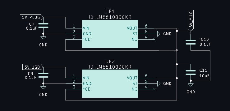
The 5V rails from both USB and the buck converter are combined using an OR-ing circuit (Dual Ideal Diodes) to prevent backfeeding before feeding the second stage of regulation.
In this configuration, the outputs of both LM66100 ideal diode controllers are tied together to form the shared 5V rail. The CE pins of each device are also tied to the output rail, ensuring both controllers are only enabled once the rail is present
This allows for testing over serial with devices that are powered by VPLUG (12V).
Voltage Regulation (II)
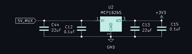
The second stage of voltage regulation involes a Low-Dropout Regulator (LDO), the MCP1826S
It is fed the combined 5V rail from the OR-ing circuit to produce the controller's logic-level voltage: 3V3
Controlled Pump Power Delivery
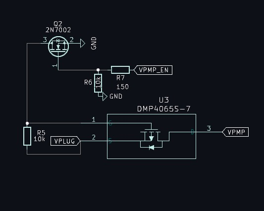
The power for the pumps is controlled using a complementary-MOSFET (CMOS) setup, driven by a digital HIGH from the S3.
Voltage Sensing
A resistor divider circuit is used to produce a signal to be read by the S3's internal ADC.
$$ R_2 = \frac{R_1 \cdot V_{out}}{V_{batt} - V_{out}} $$
$$ R_2 = \frac{100,000 \cdot 2}{12 - 2} = 20,\mathrm{k\Omega} $$
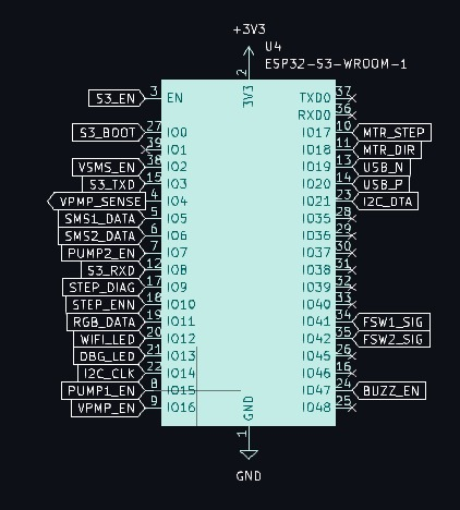
The controller is driven by an ESP32-S3-WROOM microcontroller.
Digital IO
Mode Select and Reset Toggle
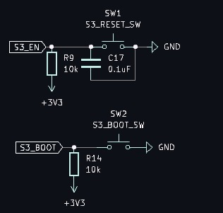
The S3 can be put into BOOT mode and RESET with onboard buttons.
BOOT mode determines whether the chip runs existing code from flash memory or waits to download new firmware.
GPIO0) during reset to determine the boot mode.10kΩ pull-up resistor to ensure a defined high state during normal operation.| BOOT0 Level | Boot Mode |
|---|---|
| HIGH | Programming Mode |
| LOW | Memory Mode |
RESET controls the Enable (EN) pin which is the ON/OFF (reset) switch for the ESP32.
1µF capacitor to filter out button noise.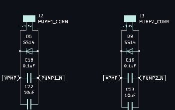 | 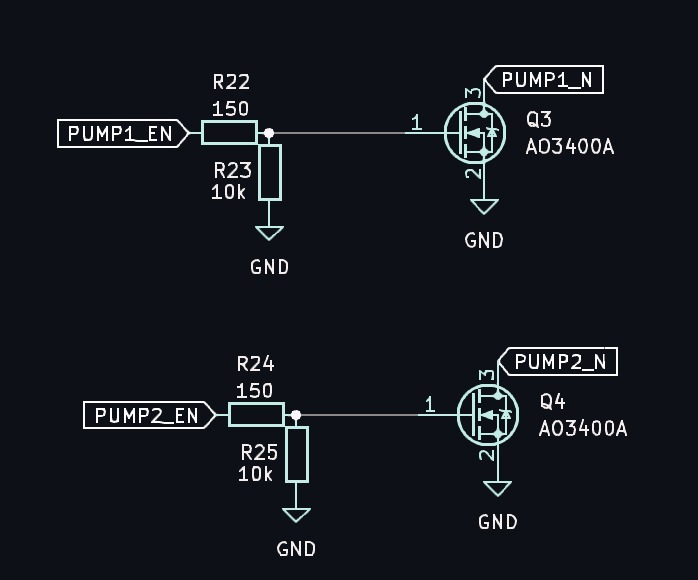 |
The controller interfaces with 12V 300mA rated pumps for irrigation.
These pumps connect via JST-XH vertical headers and are met with flyback diodes for inductive spike protection, and decoupling to filter out noise.
Each pump is controlled by a low-side switch using an A03400A N-channel MOSFET.
This will bridge the negative pump terminal to GND and effectively turn it ON when the gate is HIGH.
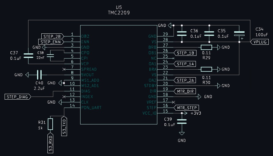
The controller interfaces with a NEMA 17 stepper motor through a TMC2209 driver for blind control.
The NEMA 17 stepper motor connects via a vertical 4-position JST-XH header.
The positive and negative terminals of both stepper coils feed the OBX and OAX pins of the driver.
The driver is powered by VPLUG and is decoupled for bulk and high-frequency noise with electrolytic and ceramic capacitors.
ENN pin to avoid power consumption, which is why I didn't use a CMOS/controlled-power delivery setup.The main control signals are STEP and DIR, controlling the speed and direction, respectively. These connect digital pins on the S3.
The single-wire UART interface was used for advanced chip config, live diagnostics, and features.
The BRA and BRB connect to 0.11Ω sense resistors to monitor and regulate current through the motor coils.
For addressing, the MS1_AD01 and MS2_AD1 pins are pulled low to set the binary address bits to 00 and the UART slave address to %0.
The CP0 and CP1 pins are tied together with a 22nF capacitor to generate a boost voltage for the internal charge pump. This boosted voltage switches the internal N-channel MOSFETs fully on.
Sensors

The controller interfaces with two capactive soil-moisture sensors (SMS) and an Ambient Light Sensor (ALS).
These connections are made with vertical 4-pin JST-XH headers.
I designed the ALS breakout board, in the future I'd be interested in designing the moisture sensors. For now I'm using the Adafruit models.
The 3V3 SMS power is controlled through a simple A03407A P-channel mosfet, and the signals are filtered with a resistor-capacitor network at the S3 ADC pins.
The ALS communicates with the I2C protocol and is powered by 3V3.
The two analog signals and I2C clock and data signals are ESD-protected by a TPD43001 TVS diode array.
Float Switches
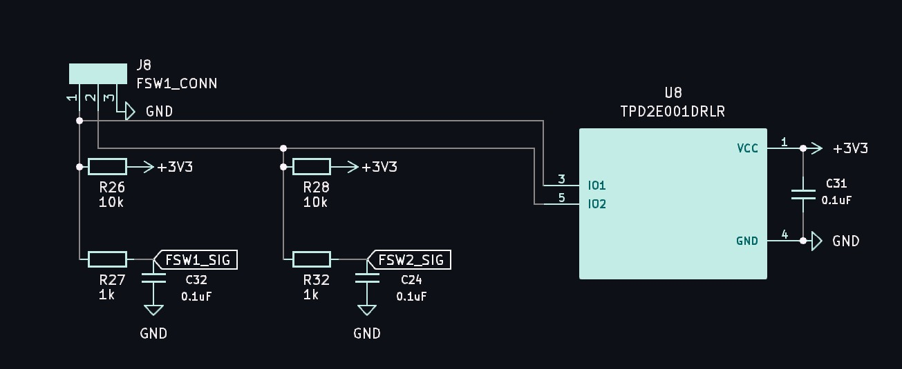
The controller interfaces with two float switches.
These connections are made with a vertical 3-pin JST-XH header.
The signals are pulled up to 3V3 to establish a defined logic stateand filtered with a resistor-capacitor network at the S3 ADC pins.
Indicator Components
This section provides insight on the mechanical components of homectrl.
I used Fusion360 to design everything.
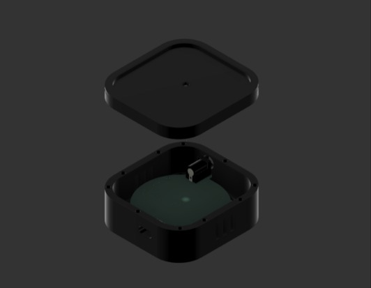
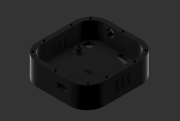
The container uses a rounded-rectangular exterior to house the board.
The board is mounted using M2 standoffs designed from the base of the container.
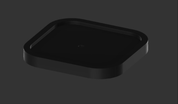
The lid is mounted magnetically on the outer top face of the container using projected holes for small magnets.
huge thanks to PCBWay for sponsoring this project's first revision.
check out REV A
Jeevan Sanchez, 2026
| Qty | Value | Footprint | References |
|---|---|---|---|
| 25 | 0.1uF | Capacitor_SMD:C_0402_1005Metric | C10, C12, C14, C15, C17, C20, C21, C24, C25, C26, C27, C28, C29, C30, C31, C32 +9 |
| 11 | 10k | Resistor_SMD:R_0402_1005Metric | R4, R5, R6, R9, R14, R19, R23, R25, R26, R28, R33 |
| 9 | 150 | Resistor_SMD:R_0402_1005Metric | R7, R13, R15, R16, R17, R18, R22, R24, R36 |
| 5 | 1k | Resistor_SMD:R_0402_1005Metric | R27, R31, R32, R39, R40 |
| 4 | 10uF | Capacitor_SMD:C_0603_1608Metric | C11, C16, C22, C23 |
| 4 | 22uF | Capacitor_SMD:C_0805_2012Metric | C6, C13, C42, C44 |
| 3 | 4.7k | Resistor_SMD:R_0402_1005Metric | R1, R34, R35 |
| 3 | AO3400A | Package_TO_SOT_SMD:SOT-23 | Q3, Q4, Q5 |
| 2 | clipboard:fc8df92e-a3b3-4f73-a46e-2aabbf2af471 | , | |
| 2 | 0.11 | Resistor_SMD:R_0603_1608Metric | R29, R30 |
| 2 | 0.1uF | Capacitor_SMD:C_0603_1608Metric | C18, C19 |
| 2 | 1.8K | Resistor_SMD:R_0402_1005Metric | R12, R37 |
| 2 | 100uF | EEH_ZK1V101XP:CAP_EEHZK1V101XP | C1, C34 |
| 2 | 10uF | Capacitor_SMD:C_0805_2012Metric | C2, C3 |
| 2 | 5.1k | Resistor_SMD:R_0402_1005Metric | R20, R21 |
| 2 | ID_LM66100DCKR | Package_TO_SOT_SMD:SOT-363_SC-70-6 | UE1, UE2 |
| 2 | LOGO | LOGO | G***, G*** |
| 2 | MountingHole | MountingHole:MountingHole_2.2mm_M2 | H1, H2 |
| 2 | PLUG_LED | LED_SMD:LED_0603_1608Metric | D2, D7 |
| 2 | SS14 | Diode_SMD:D_SMA | D5, D9 |
| 1 | 100k | Resistor_SMD:R_0603_1608Metric | R2 |
| 1 | 100k | Resistor_SMD:R_0402_1005Metric | R8 |
| 1 | 10nF | Capacitor_SMD:C_0402_1005Metric | C4 |
| 1 | 10uH | Inductor_SMD:L_Changjiang_FNR6045S | L1 |
| 1 | 2.2uF | Capacitor_SMD:C_0402_1005Metric | C40 |
| 1 | 20K | Resistor_SMD:R_0402_1005Metric | R11 |
| 1 | 22nF | Capacitor_SMD:C_0402_1005Metric | C38 |
| 1 | 2N7002 | Package_TO_SOT_SMD:SOT-23 | Q2 |
| 1 | 3.3nF | Capacitor_SMD:C_0402_1005Metric | C8 |
| 1 | 3A 24V PTC | Fuse:Fuse_1812_4532Metric | F1 |
| 1 | 3V3_LED | LED_SMD:LED_0603_1608Metric | D8 |
| 1 | 3V3_TP_PAD | TestPoint:TestPoint_Pad_1.5x1.5mm | TP2 |
| 1 | 470 | Resistor_SMD:R_0402_1005Metric | R10 |
| 1 | 50k | Resistor_SMD:R_0402_1005Metric | R3 |
| 1 | 5V_BATT_TP_PAD | TestPoint:TestPoint_Pad_1.0x1.0mm | TP6 |
| 1 | 5V_MUX_TP_PAD | TestPoint:TestPoint_Pad_1.0x1.0mm | TP8 |
| 1 | 5V_USB_TP_PAD | TestPoint:TestPoint_Pad_1.0x1.0mm | TP4 |
| 1 | ALS_CONN | Connector_JST:JST_XH_B4B-XH-A_1x04_P2.50mm_Vertical | J7 |
| 1 | AO3407A | Package_TO_SOT_SMD:SOT-23 | Q1 |
| 1 | BAT54J | Diode_SMD:D_SOD-323F | D13 |
| 1 | Barrel_Jack | Connector_BarrelJack:BarrelJack_Horizontal | J1 |
| 1 | CMT-0525-75-SMT-TR | CMT_0525_75_SMT_TR:XDCR_CMT-0525-75-SMT-TR | BZ1 |
| 1 | DBG_LED | LED_SMD:LED_0603_1608Metric | D11 |
| 1 | DMP4065S-7 | Package_TO_SOT_SMD:SOT-23 | U3 |
| 1 | ESP32-S3-WROOM-1 | ESP32-S3-WROOM-1-N16R2:XCVR_ESP32-S3-WROOM-1-N16R2 | U4 |
| 1 | FSW1_CONN | Connector_JST:JST_XH_B3B-XH-A_1x03_P2.50mm_Vertical | J8 |
| 1 | FerriteBead | Resistor_SMD:R_1206_3216Metric | FB1 |
| 1 | GND_B_PAD | TestPoint:TestPoint_Pad_1.0x1.0mm | TP9 |
| 1 | GND_TP_DRILL | TestPoint:TestPoint_THTPad_D1.0mm_Drill0.5mm | TP3 |
| 1 | GND_TP_PAD | TestPoint:TestPoint_Pad_1.5x1.5mm | TP1 |
| 1 | MCP1826S | Package_TO_SOT_SMD:SOT-223-3_TabPin2 | U2 |
| 1 | MMSZ5243BT1G | Diode_SMD:D_SOD-123 | D3 |
| 1 | ON_LED | LED_SMD:LED_0603_1608Metric | D10 |
| 1 | PUMP1_CONN | Connector_JST:JST_XH_B2B-XH-A_1x02_P2.50mm_Vertical | J2 |
| 1 | PUMP2_CONN | Connector_JST:JST_XH_B2B-XH-A_1x02_P2.50mm_Vertical | J3 |
| 1 | S3_BOOT_SW | TACT_TS1185:SW_5-B-B-B-A_XKB | SW2 |
| 1 | S3_RESET_SW | TACT_TS1185:SW_5-B-B-B-A_XKB | SW1 |
| 1 | SI2347DS-T1-GE3 | Si2347DS:SOT_7DS-T1-GE3_VIS | U9 |
| 1 | SMAJ14A | Diode_SMD:D_SMA | D1 |
| 1 | SMS1_CONN | Connector_JST:JST_XH_B4B-XH-A_1x04_P2.50mm_Vertical | J6 |
| 1 | SS34 | Diode_SMD:Nexperia_CFP3_SOD-123W | D4 |
| 1 | STEP_CONN | Connector_JST:JST_XH_B4B-XH-A_1x04_P2.50mm_Vertical | J4 |
| 1 | SYS_LED | LED_SMD:LED_WS2812B-Mini_PLCC4_3.5x3.5mm | D14 |
| 1 | TMC2209 | ul_TMC2209:QFN28_5X5_TRI | U5 |
| 1 | TPD2E001DRLR | TPD2E001DRLR:SOT50P160X60-5N | U8 |
| 1 | TPD4E001DRLR | Package_TO_SOT_SMD:Texas_R-PDSO-N6_DRL-6 | U7 |
| 1 | TPS5405DR | TPS5405DR:SOIC127P599X175-8N | U1 |
| 1 | USB_C_CONN | Connector_USB:USB_C_Receptacle_G-Switch_GT-USB-7010ASV | J5 |
| 1 | USB_LED | LED_SMD:LED_0603_1608Metric | D6 |
| 1 | VPLUG_TP_DRILL | TestPoint:TestPoint_THTPad_D1.0mm_Drill0.5mm | TP5 |
| 1 | VPLUG_TP_PAD | TestPoint:TestPoint_Pad_1.0x1.0mm | TP7 |
| 1 | VPMP_LED | LED_SMD:LED_0603_1608Metric | D15 |
| 1 | WIFI_LED | LED_SMD:LED_0603_1608Metric | D12 |
It measures 63.2 × 70.5 mm and has 4 copper layers, 1.6 mm thick.
141 parts, built around the ESP32-S3-WROOM-1-N8, DMP4065S-7, SI2347DS-T1-GE3-1 and TMC2209. The full list of its parts is on this page, with links to each part's symbol and footprint where PCBKit's library has them.
From the jeevan9s/homectrl-sys repository on GitHub, at the commit this page was made from: the board is hardware/homectrl-v2/homectrl-v2.kicad_pcb and its schematic hardware/homectrl-rB/ESP-breakout.kicad_sch. PCBKit opens the board in the browser, with nothing to install.
Its repository states no licence, so its author keeps all rights: ask jeevan9s before reusing the design.


Spaceflight-Rocketry-Giessen-e-V/Telemetry
Open-Source Rocket Telemetry System Based On Radiocrafts RC232 Radio Modules

icl-rocketry/Ricardo-PickleRick
A more compact Ricardo classic featuring a new sensor array, 4 pyro channels and 4 servo channels. Includes Ricardo bus plug too.


SaikoJuanma/phone_replacement
this projects aims to create a replacement for the phone, so I can stop using my phone on the home and get rid off distractions. ## Upcoming features 1. Timer and alarm. 2. PCB and schematics for the project. 3.


