4 layers118 × 60 mm
 jbilander/Base6433
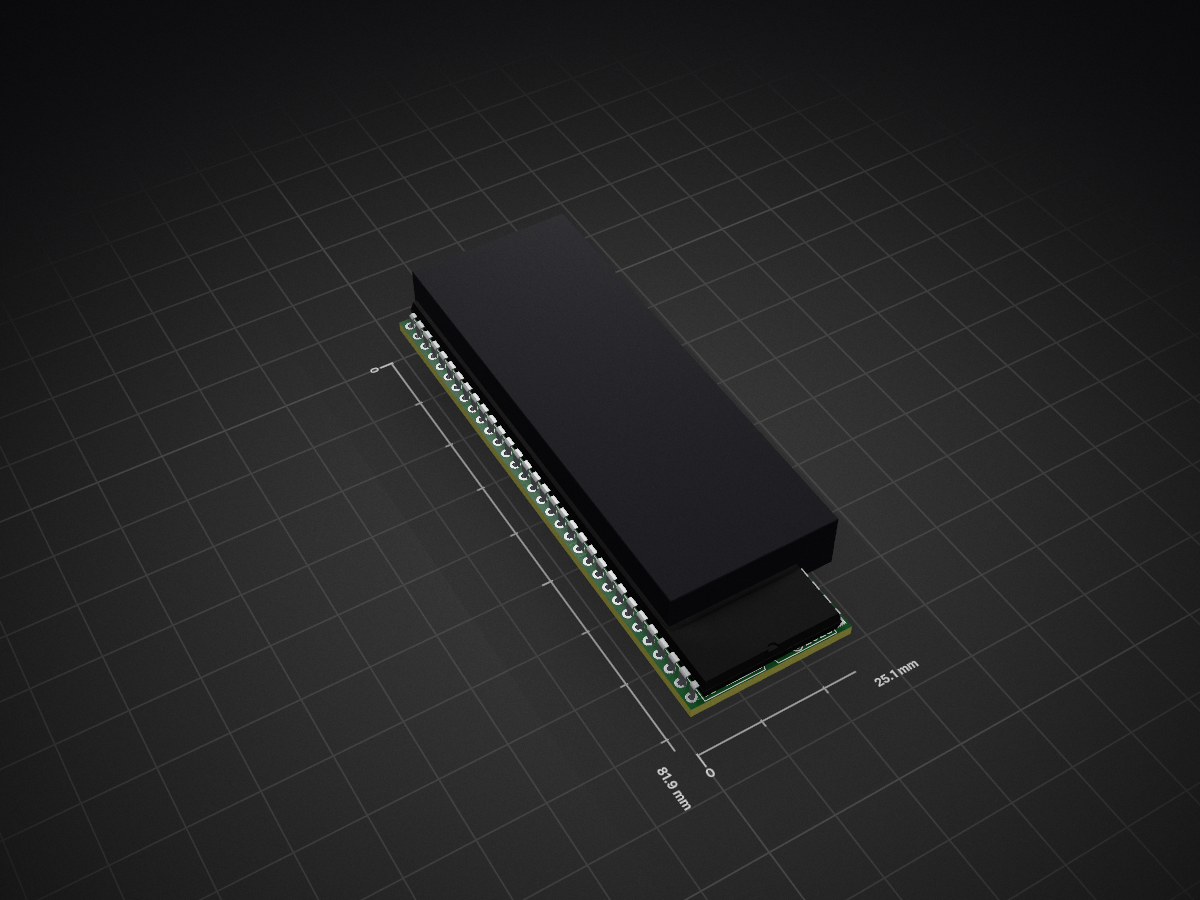
A 68k carrier board in DIP-64 that takes the iCESugar-Pro-v1.3 FPGA module
Base64 is an open-source printed circuit board by jbilander, from the jbilander/Base64 repository on GitHub, published under the CC-BY-SA-4.0 licence. It is a 4-layer board of 25.1 × 81.9 mm with 34 parts on 266 nets, routed with 1,109 tracks and 153 vias.
It is built around the 570BLFT, SN74LVC1G17DBVR and TLV75533PDBVR-MS. Its parts include 11 capacitors, 11 ICs, 5 resistors and 2 connectors. It belongs with the fPGA and programmable logic boards of this library.


A 68k carrier board in DIP-64 that takes the iCESugar-Pro-v1.3 FPGA module


Contents
The host system provides a 7.09 MHz reference (E-clock derivative) on the CPU socket pin 15. This is buffered by the 74LVC1G17 Schmitt-trigger gate (powered from the local 3.3 V rail, with 5 V-tolerant inputs) and routed both to the FPGA at PT27A (C7, PCLKT0_1/+) and to the ICS570B zero-delay clock multiplier (configured for 12× via floating S0/S1 with CLK/2 feedback).
The 570B produces a phase-aligned 84 MHz on CLK and 42 MHz on CLK/2. The 84 MHz output feeds the FPGA at PL26A (L1, PCLKT6_1/HS+), which is well above the ECP5's 8 MHz PFD minimum and locks reliably to the on-chip PLL. Inside the FPGA, the 84 MHz is divided down to produce turbo CPU clocks (14 / 21 / 28 / 42 MHz) that remain phase-aligned to the original 7 MHz reference.
The Base64 carrier board requires an iCESugar-Pro v1.3 FPGA module by Muse Lab, which mounts into the SO-DIMM socket (J1). The module carries the Lattice ECP5 LFE5U-25F-6BG256C FPGA along with onboard 32 MB SDRAM, 32 MB SPI flash, and an iCELink USB-C programmer.
Available from the official Muse Lab AliExpress store.
| Ref | Qty | Value / Part | Description | Package | Mouser P/N |
|---|---|---|---|---|---|
| U1 | 1 | ICS570BLFT | Zero-delay clock multiplier with feedback (12× config) | SOIC-8 | 972-570BLFT |
| U2–U8 | 7 | SN74CBTD3861DGVR | 10-bit FET bus switch with 5 V→3.3 V diode level shift | TVSOP-24 | 595-SN74CBTD3861DGVR |
| U9 | 1 | SN74LVC1G17DBVR | Single Schmitt-trigger buffer, 5 V-tolerant inputs | SOT-23-5 | 595-SN74LVC1G17DBVR |
| U10 | 1 | TLV75533PDBVR | 3.3 V LDO regulator, 500 mA, fixed output | SOT-23-5 | 595-TLV75533PDBVR |
| C1 | 1 | 1 µF | LDO input cap, X7R, 25 V | 0805 | 187-CL21B105KAFNNNE |
| C2–C10 | 9 | 100 nF | CBTD / buffer / LDO output decoupling, X7R, 50 V | 0603 | 187-CL10B104KA8NNNC |
| C11 | 1 | 10 nF | 570B VDD decoupling (per datasheet), X7R, 50 V | 0603 | 187-CL10B103KA8WPNC |
| R1–R2 | 2 | 33 Ω | Series termination, 1% | 0805 | 652-CR0805FX-33R0ELF |
| R3–R4 | 2 | 33 Ω | Series termination, 1% | 0603 | 652-CR0603FX-33R0ELF |
| R5 | 1 | 10 kΩ | Autoconfig /CFGIN pull-up, 1% | 0603 | 652-CR0603FX-1002ELF |
| J1 | 1 | TE 1473149-4 | 200-pin SO-DIMM (DDR2) socket for FPGA module | SMT | 571-1473149-4 |
| J2 | 1 | 3-pin right-angle header | Autoconfig header (/CFGOUT, /CFGIN, GND), 0.64 mm square, 2.54 mm pitch | THT | AliExpress |
| U11 | 2 | 40-pin breakaway male pin strip, 2.54 mm pitch | Round pins, ~11.96 mm overall pin length, used as DIP-64 CPU socket pins | THT | AliExpress |
U11 (CPU socket pins): these are round male pins supplied as 40-pin breakaway pin strips on 2.54 mm pitch, with ~11.96 mm overall pin length (top of pin to bottom). Break each strip down to a 32-pin section — you need two such sections, so two strips minimum. See step 8 of the build guide for fitting them.
J2 (autoconfig header):
This header supports Amiga-style autoconfig daisy-chaining, and autoconfig is implemented and working in the current FPGA designs. J2 is therefore not optional — it has to be wired one of these two ways:
If neither connection is made, R5 holds /CFGIN high, the board waits for its turn in the chain that never comes, and it will not appear to the system.
For use in non-Amiga 68k systems, J2 is not applicable in its standard form, though it could potentially be repurposed depending on the target system.
J2 uses a standard 0.64 mm square 2.54 mm pitch right-angle pin header. Available from AliExpress directly as a 3-pin part, or cut from a 40-pin breakaway strip.
This is how I build the board: everything hand-placed and hand-soldered, then a single pass through a desktop reflow oven to even out the joints, and finally the through-hole parts. It is not the only way to do it — see alternative approaches if you are building more than one or two boards — but it needs no stencil and no paste, and it gives a clean, repeatable result.
Everything below assumes leaded solder. If you use lead-free you will need a correspondingly hotter reflow profile.
| Soldering iron | Temperature-controlled, with a 1 mm tip for the SO-DIMM pins |
| Solder (SMD + pins) | Stannol 518644 Sn60Pb40, 0.5 mm |
| Solder (GND pads) | Sn60Pb40, 1 mm |
| High-power iron | ZD-915 desoldering station, or any iron with enough thermal mass for a large ground pour |
| Reflow oven | T-962 desktop IR oven, or equivalent (hot plate / hot air with a proper profile) |
| Flux | No-clean flux, paste or pen |
| Kapton tape | For masking parts during high-heat steps |
| Cleaning | IPA, cotton buds, plus an electronics cleaner for the ICs (see step 7) |
| Inspection | Microscope or a decent magnifier |
Work in the order C2, U2, C3, U3, C4, U4 … C8, U8 — one capacitor, then the IC it decouples, then the next pair.
It is tempting to place all the capacitors in a single pass, but C2–C8 sit right next to the drag-solder path along U2–U8. With all of them already fitted, drag-soldering the TVSOP-24 packages becomes much more awkward. Alternating keeps the area around each IC clear when you need it.
With the bus switches down, solder the resistors (R1–R5) and the remaining capacitors (C1, C9, C10, C11). Then fit the three remaining ICs: U9 (Schmitt buffer), U10 (LDO) and U1 (clock multiplier).
Once all other surface-mount parts are on, place the SO-DIMM socket. There is a little wiggle room in the footprint, so take the time to align and centre it as well as you can against the silkscreen before tacking it down. Tack one corner, re-check the alignment along the whole length, then tack the opposite corner.
I solder these pin by pin rather than drag-soldering. The socket contacts are fine and springy, and a drag tip tends to bend and flex them, which makes bridges easy and a clean result hard.
Instead: use a 1 mm tip, flux the pins, pick up a small blob of solder on the tip and transfer it to a pin — or two pins at a time once you find a rhythm. It is tedious, there is no way around that. What matters is that every pin ends up with a small but definite amount of solder on it.
Don't worry if the row looks uneven at this stage. The reflow step later will sort it out.

Hand-soldering the 200 pins with 0.5 mm Sn60Pb40. Uneven at this point — that is expected.
The socket's two metal retention arms land on large ground pours, which sink far more heat than a normal iron can deliver. I use the ZD-915 desoldering station for this because it has the thermal capacity; a large chisel tip on a high-power iron will also work.
Be careful not to let the nozzle rest against the connector body — the plastic will melt. As with the pins, the joint does not need to look pretty yet.

ZD-915 at 360 °C on the ground pad, with U8 and R5 masked off under kapton tape.
At this point everything except the through-hole parts is soldered. Clean the spent flux off the board, apply a fresh coat, and run it through the oven.
I use a T-962 desktop IR oven with the Amtech SynTECH-LF profile, which ramps to a 240 °C peak and then cools down.

Two boards loaded in the T-962.

The Amtech SynTECH-LF profile as shown on the T-962.
Gravity and surface tension do the rest — joints that looked lumpy going in come out even.
Inspect every pin under magnification: each should have a clean fillet, and there should be no bridges anywhere along the socket.
Then clean the board with cotton buds and IPA.
For the ICs, don't use neat IPA — it lifts the laser marking off the packages. I use a general-purpose electronics cleaner instead, with the compound:
Hydrocarbons, C6-C7, n-alkanes, isoalkanes, cyclics, <5 % n-hexane, 2-Propanol
Applied to a clean cotton bud and wiped gently over the package, this cleans the ICs without erasing the text the way 100 % IPA does.

Electronics cleaner used on the ICs — cleans without taking the markings with it.

Two boards after reflow and cleanup.
Last come the two 32-pin strips (U11) and the 3-pin CFG header (J2). Fit J2 — it is required for the board to autoconfig, and you will need a jumper shunt for it unless you are daisy-chaining from another device. See notes on selected parts.
Push each 32-pin section through the carrier board pads from the underside and solder on the top side. The protruding bottom side is what plugs into the host system's MC68000 socket.
The 32-pin sections are broken out of cheap 40-pin breakaway strips, and the break leaves a rougher edge on that end. It makes no difference electrically, but it is a nice touch to orient both strips so the clean edges face the same way — which of course puts both rough edges on the other side.

Clean edges on the same side …

… and the two broken edges together on the other.
Finish with a final clean of the through-hole joints using cotton buds and IPA to remove the excess flux.
Hand-soldering the 200 pins is the slow way. Two alternatives worth considering:
On my own iCESugar-Pro module I found a mark on the 25 MHz crystal oscillator that looks like it may have been made by a pin during installation of the module. I can't say for certain where the dent came from, or whether it is a problem at all — it is worth a look under a microscope if you have one. As a precaution I put a piece of kapton tape over the oscillator.

Kapton tape over the 25 MHz oscillator on the iCESugar-Pro module.
Amiga autoconfig is implemented and working in the current FPGA designs — see the J2 notes for the jumpering it requires.
Rev C changes vs Rev B:
| Qty | Value | Footprint | References |
|---|---|---|---|
| 9 | 100nF | Capacitor_SMD:C_0603_1608Metric | C2, C3, C4, C5, C6, C7, C8, C9, C10 |
| 7 | SN74CBTD3861DGVR | Package_SO:TSSOP-24_4.4x5mm_P0.4mm | U2, U3, U4, U5, U6, U7, U8 |
| 2 | 33 | Resistor_SMD:R_0805_2012Metric | R1, R2 |
| 2 | 33 | Resistor_SMD:R_0603_1608Metric | R3, R4 |
| 1 | 10k | Resistor_SMD:R_0603_1608Metric | R5 |
| 1 | 10nF | Capacitor_SMD:C_0603_1608Metric | C11 |
| 1 | 1473149-4 | Base64:TE_DDR2-SODIMM-200_1473149-x | J1 |
| 1 | 1uF | Capacitor_SMD:C_0805_2012Metric | C1 |
| 1 | 570BLFT | Package_SO:SOIC-8_3.9x4.9mm_P1.27mm | U1 |
| 1 | 68000_PinHeader | Package_DIP:DIP-64_W22.86mm | U11 |
| 1 | Conn_01x03 | Connector_PinHeader_2.54mm:PinHeader_1x03_P2.54mm_Horizontal | J2 |
| 1 | SN74LVC1G17DBVR | Base64:SOT95P280X145-5N | U9 |
| 1 | TLV75533PDBVR | Package_TO_SOT_SMD:SOT-23-5 | U10 |
The 29 most common of 34 parts.
It measures 25.1 × 81.9 mm and has 4 copper layers, 1.6 mm thick.
34 parts, built around the 570BLFT, SN74LVC1G17DBVR and TLV75533PDBVR-MS. The full list of its parts is on this page, with links to each part's symbol and footprint where PCBKit's library has them.
From the jbilander/Base64 repository on GitHub, at the commit this page was made from: the board is KiCad/Base64.kicad_pcb. PCBKit opens the board in the browser, with nothing to install.
Its repository publishes it under the CC-BY-SA-4.0 licence: you may reuse it on that licence's terms (keep the author's notice, and for a copyleft licence share your changes alike).

Matrixite/MatrixDrive
MatrixDrive is a USB-loadable Mega Drive/Genesis cartridge

techmannih/pd1180-epr
PD1180-EPR — NEMA 34 Smart Motor-Mounted Stepper Controller with USB-C PD 3.1 EPR

mx3353672833-debug/moto-gps-waveshare
MOTO GPS · Waveshare ESP32-S3 1.75C 圆屏导航 + iPhone App | Author: Maler X | Noncommercial, attribution required | Experimental

theohg/PD240W
PD240W is a complete hardware and firmware project converting USB-C Power Delivery into a programmable 240W (48V 5A) bench power supply, featuring C++ code for Raspberry Pi Pico, custom PCB Gerbers, and a 3D-printable…

Guilleloma/Furby-GPT
This project transforms a 1998 Furby into an interactive and advanced desktop assistant using a Raspberry Pi W. It incorporates OpenAI and Whisper for natural language processing, primarily relying on Google Cloud Text…

fl4p/Fugu2
Links: git | kicanvas | cadlab | docs | pdf schematics | IBOM (TODO) | firmware | additional docs & resources
