
4 layers234 × 84 mm
Main panel
google/mozc-devices
Circuit diagrams and firmware source code for Gboard DIY keyboards
234 parts3kApache-2.0

 j-w-e/wysteria33
custom split keyboard
Wysteria is an open-source printed circuit board by j-w-e, from the j-w-e/wysteria repository on GitHub. It is a 2-layer board of 158.2 × 115.1 mm with 84 parts on 60 nets, routed with 1,051 tracks and 6 vias.
It is built around the SK6812MINI-E. Its parts include 21 diodes, 18 switches and 18 inductors. It belongs with the keyboards and input boards of this library.
This is my custom split 36-key keyboard, with an encoder knob on each hand, and a pinky cluster to avoid stretching my pinky – I find lateral movement easier.
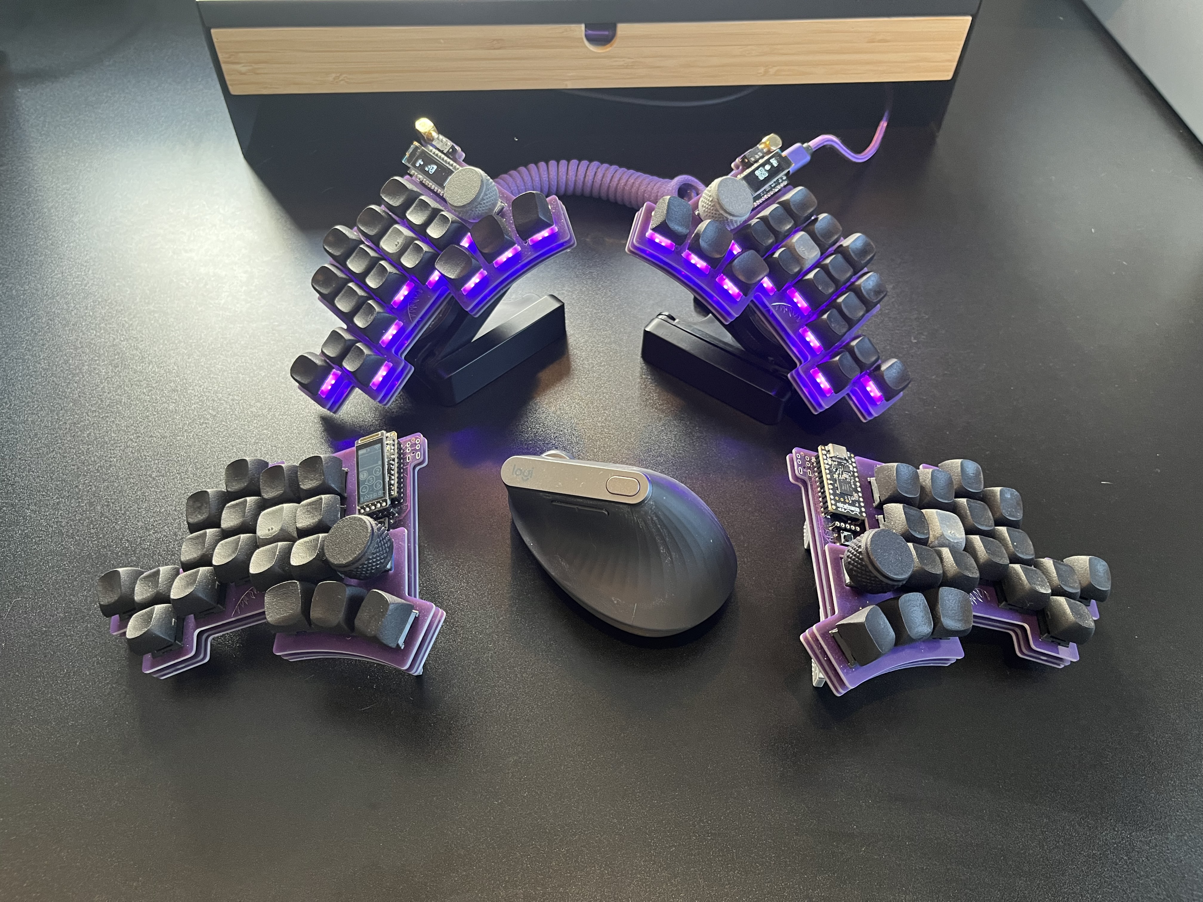
The pcbs, and the source ergogen file used to generate v0.3, can be found in the pcbs folder.
It has working firmware for both QMK and ZMK. Source files are in the repo, but I have not put this into the main repos for either QMK or ZMK. My own build process symlinks these as appropriate.
v0.3 has been printed and tested, and is my current daily driver. However, please note that to build it, the diodes on the thumb cluster need to be handwired to the rows. The traces on the PCB itself are incorrect. This has been fixed in the ergogen config file, ready for if and when I print it again, but this has not had all the traces set up in KiCad, and has not been printed or tested.
If I ever decide to build a new one, want to:
Made based on
| Qty | Value | Footprint | References |
|---|---|---|---|
| 19 | ComboDiode | D1, D2, D3, D4, D5, D6, D10, D11, D12, D13, D14, D15, D16, D17, D18, D19 +3 | |
| 18 | MX | S1, S2, S3, S4, S5, S6, S7, S10, S11, S12, S13, S14, S15, S16, S17, S18 +2 | |
| 18 | SK6812Mini-e | WS2812B | L9, L9, L9, L9, L9, L9, L9, L9, L9, L9, L9, L9, L9, L9, L9, L9 +2 |
| 2 | E73:SW_TACT_ALPS_SKQGABE010 | B1, B2 | |
| 2 | E73:SPDT_C128955 | T1, T2 | |
| 2 | output v0.2 as printed:Wysteria | D20, D20 | |
| 1 | lib:bat | JST1 | |
| 1 | ProMicro | _1 | |
| 1 | combo_display | SCREEN1 | |
| 1 | rotary_encoder | ROT1 | |
| 1 | TRRS-PJ-320A-dual | TRRS-PJ-320A-dual | TRRS1 |
The 66 most common of 84 parts.
It measures 158.2 × 115.1 mm and has 2 copper layers, 1.6 mm thick.
84 parts, built around the SK6812MINI-E. The full list of its parts is on this page, with links to each part's symbol and footprint where PCBKit's library has them.
From the j-w-e/wysteria repository on GitHub, at the commit this page was made from: the board is pcbs v0.3/pcbs/wysteria.kicad_pcb. PCBKit opens the board in the browser, with nothing to install.
Its repository states no licence, so its author keeps all rights: ask j-w-e before reusing the design.
google/mozc-devices
Circuit diagrams and firmware source code for Gboard DIY keyboards

Bastardkb/Dilemma
The Dilemma is a vertical stagger low-profile keyboard with mods.

Pwnsat/FlatSat
Flatsat v1.0 is a hardware based platform for aerospace cybersecurity research

adamws/kicad-kbplacer
KiCad plugin for automatic keyboard's key placement and routing

imchipwood/dumbpad
Simple 4x4 numpad with rotary encoder. Powered by QMK via ATmega32u4 Pro Micro

makerforgetech/modular-biped
An open source framework for creating a bipedal modular companion robot.

