2 layers102.2 × 68.2 mm
4mb mapper nms8280
iricryst/4mb-mapper-nms8280
A low-profile PCB implementation of the 4 MB memory mapper for the Philips NMS 8280 MSX2, based on the original design by Hans Oranje.
28 parts

 iricryst/4mb-mapper-nms8280
A low-profile PCB implementation of the 4 MB memory mapper for the Philips NMS 8280 MSX2, based on the original design by Hans Oranje.
4mb mapper nms8280 is an open-source printed circuit board by iricryst, from the iricryst/4mb-mapper-nms8280 repository on GitHub. It is a 2-layer board of 102.2 × 68.2 mm with 28 parts on 103 nets, routed with 918 tracks and 90 vias.
It is built around the 74LS125DC, 74LS157PC and 74LS670, with the 74LS00SC among its other parts. Its parts include 11 capacitors, 11 ICs and 1 connector.


A low-profile PCB implementation of the 4 MB memory mapper for the Philips NMS 8280 MSX2, based on the original design by Hans Oranje. The board is intended to replace the stock memory while keeping the mapper at slot 3.2, with the required connections and piggybacking arranged on the PCB instead of a large wiring harness.
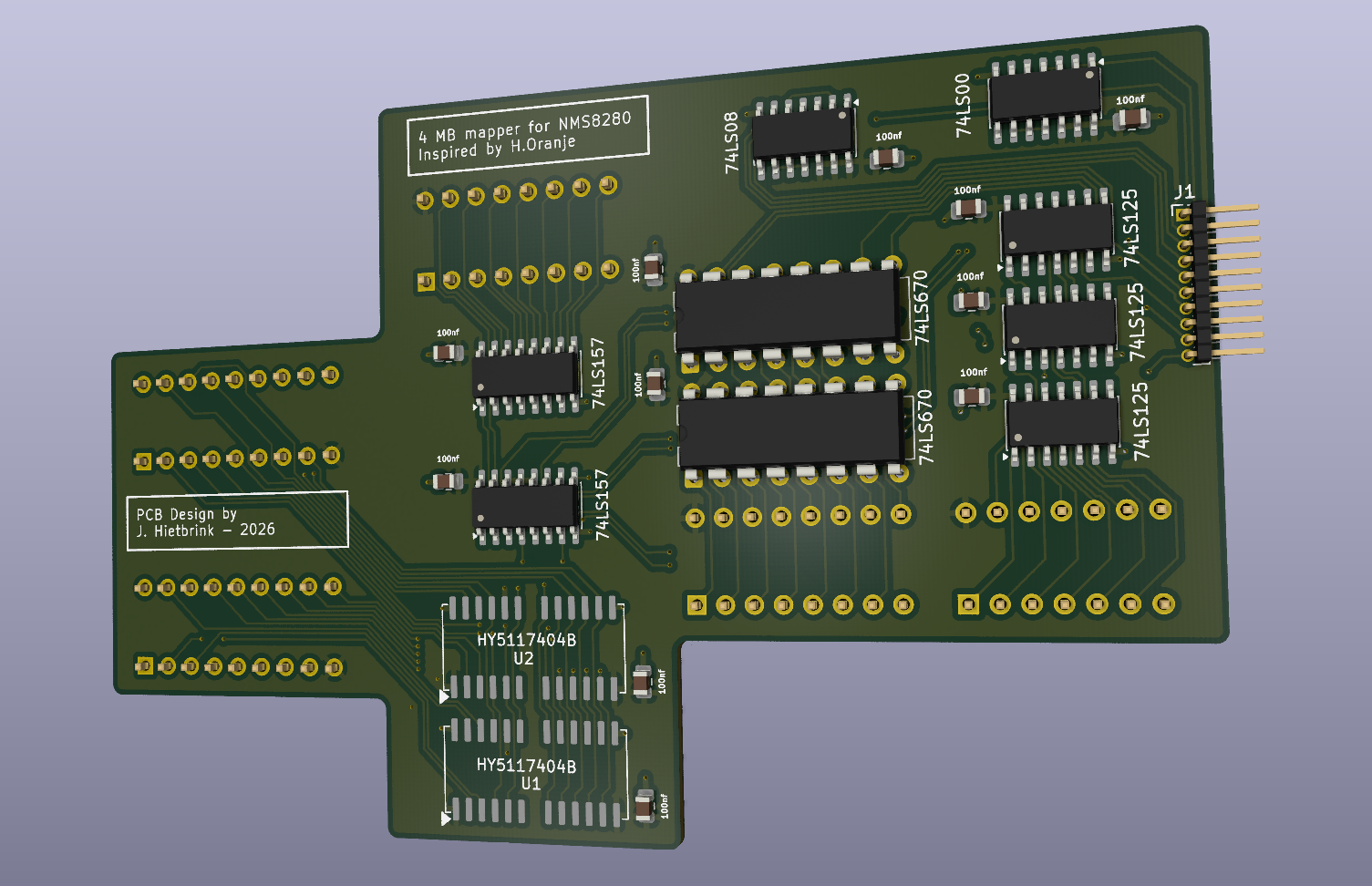
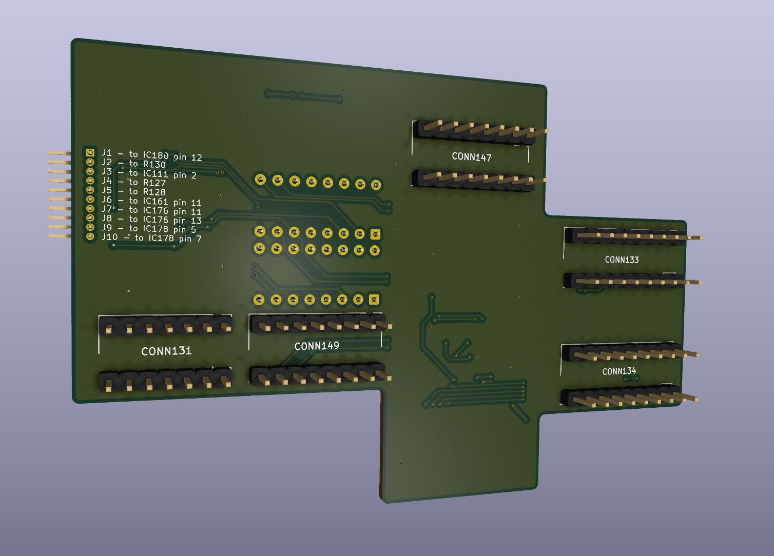
Use LS or HCT logic IC's.
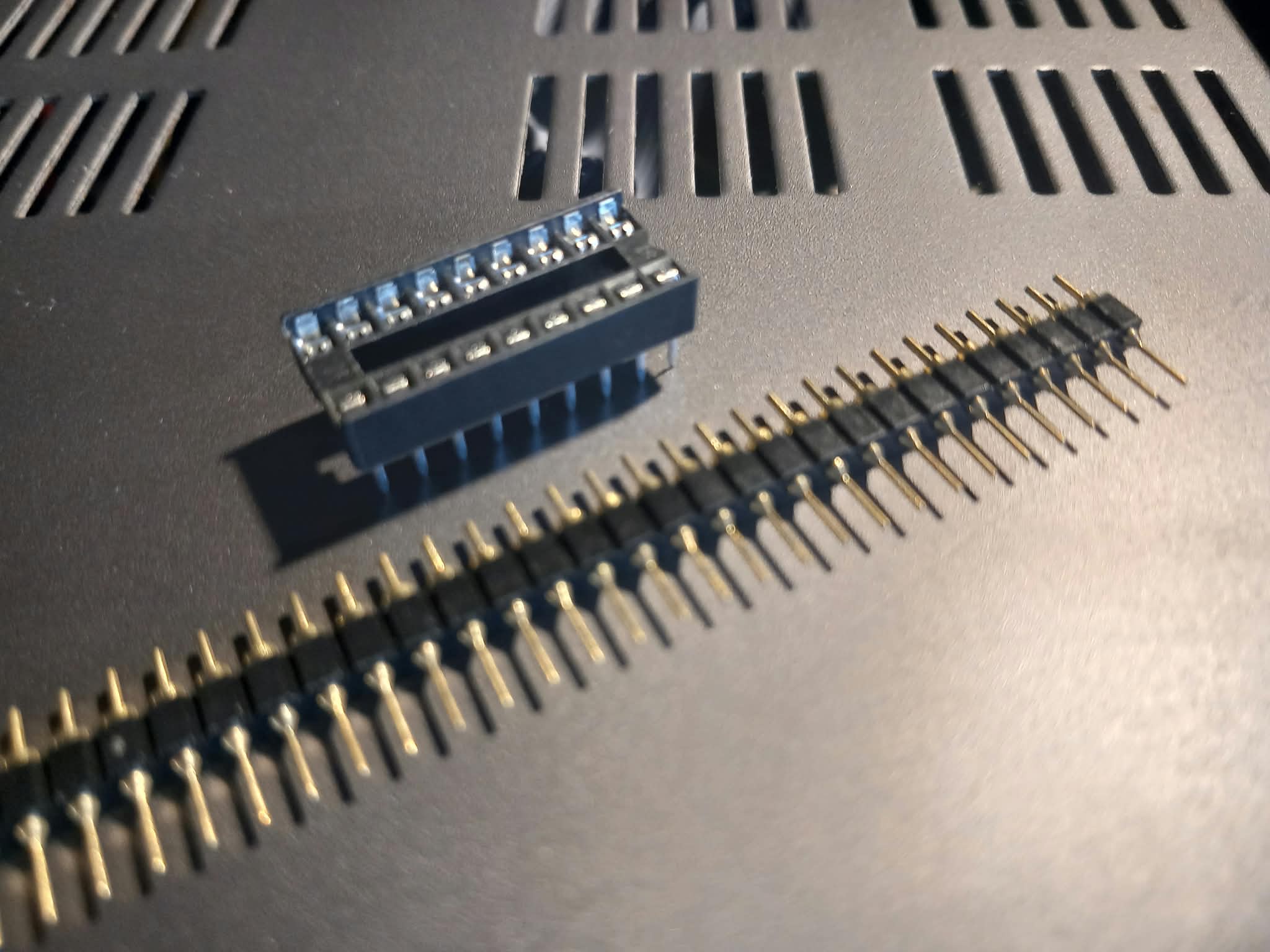
Use rounded narrow 2,54 mm pin headers
Use stamped leaf spring dip socket, with the square holes
Use above combination to overcome slight misallignment of the pins against the sockets on the mainboard.
I didn't have the exact measurements documented. And even with a caliper measurements tend be inaccurate.
Parts not described in the interactive BOM.
| Part | Amount |
|---|---|
| 2x9 2,54mm DIP Socket stamped leaf spring | 2 |
| 2x8 2,54mm DIP Socket stamped leaf spring | 2 |
| 2x7 2,54mm DIP Socket stamped leaf spring | 1 |
| 1x50 2,54mm Rounded precision pin headers | 2 |
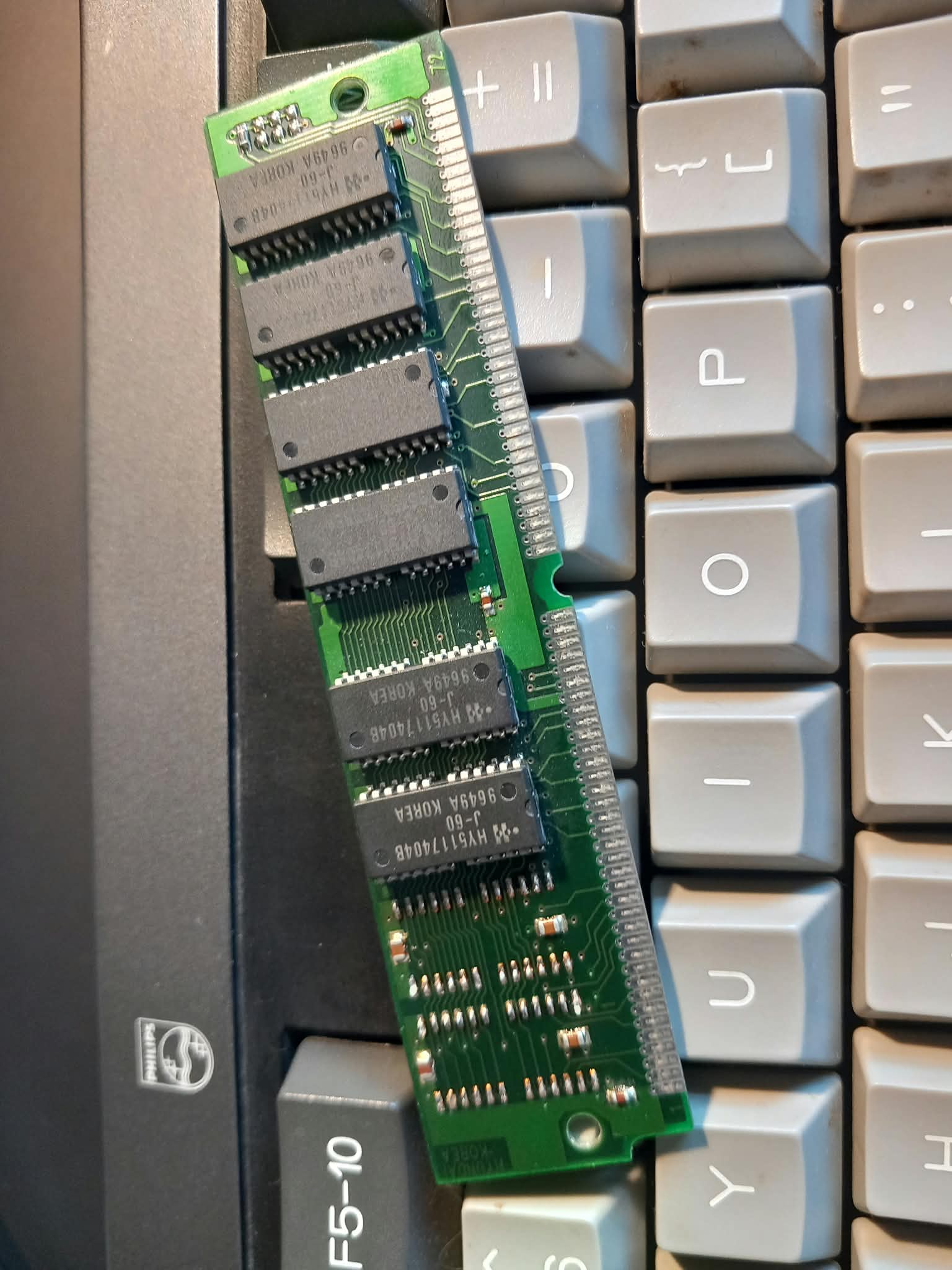
The Hyundai RAM used by this design is just wat I found in my drawer. It came of a 16 MB 72pins FPM module.
Any 4Mx4 DRAM / FPM layout will work. I used 60ns against the 120ns original RAM without, any problems.
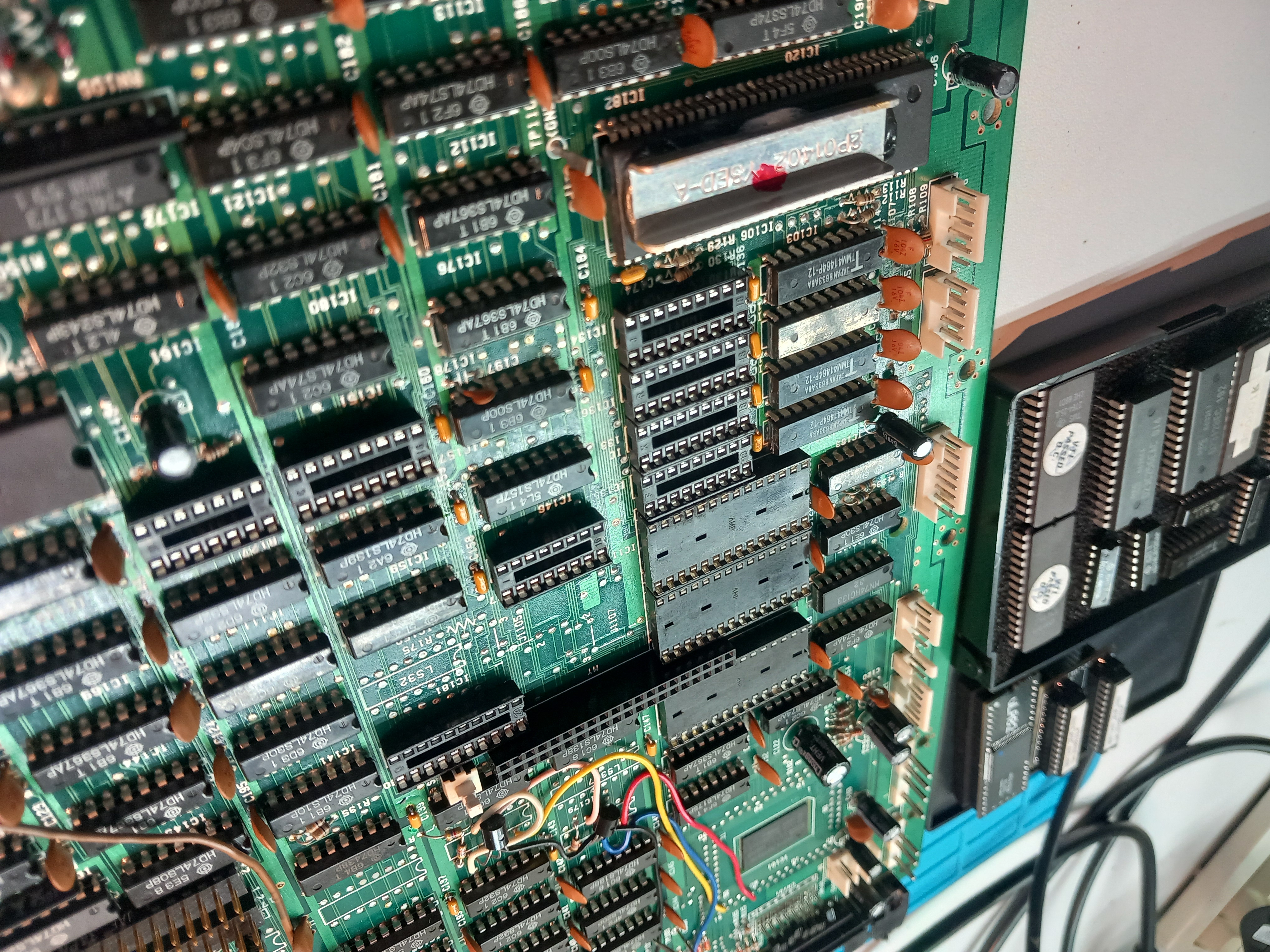
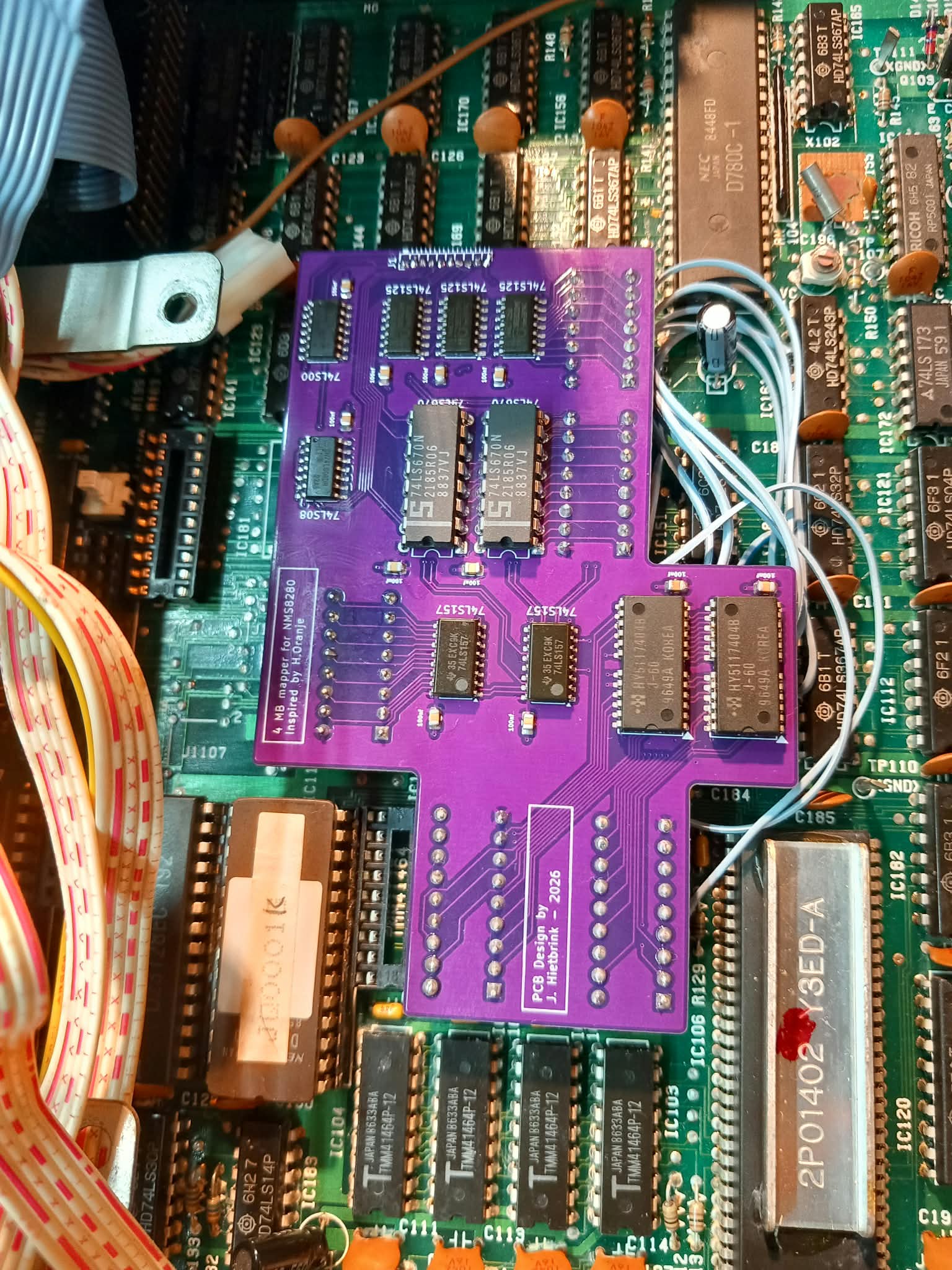
Use the cutout image as a reference for component locations. The J1 wiring points are marked with a red dot and the corresponding wire number.
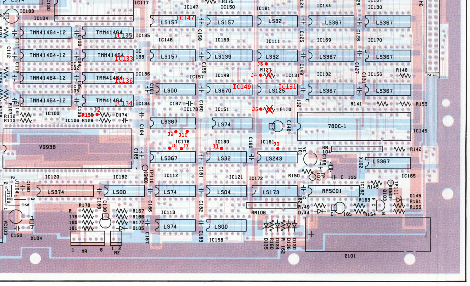
Use 30 AWG wire, or strip a floppy-disk/IDE ribbon cable.
| J1 pin | Connect to |
|---|---|
| J1 | IC180 pin 12 |
| J2 | R130, left leg when facing the mainboard as shown in the cutout image |
| J3 | IC111 pin 11 |
| J4 | R127, left pinhole when facing the mainboard as shown in the cutout image |
| J5 | R128, left pinhole when facing the mainboard as shown in the cutout image |
| J6 | IC161 pin 11 |
| J7 | IC176 pin 11 |
| J8 | IC176 pin 13 |
| J9 | IC178 pin 5 |
| J10 | IC178 pin 7 |
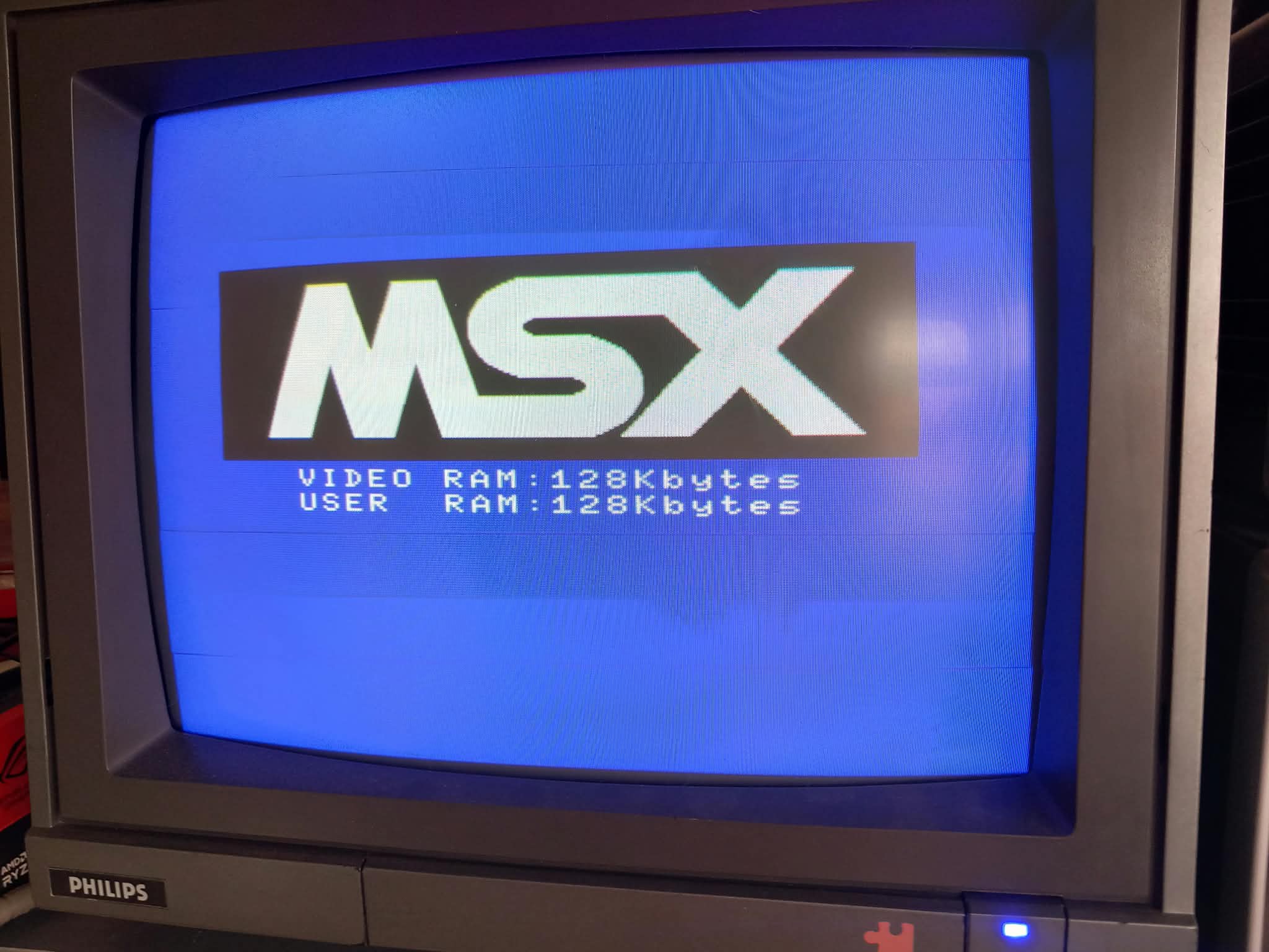
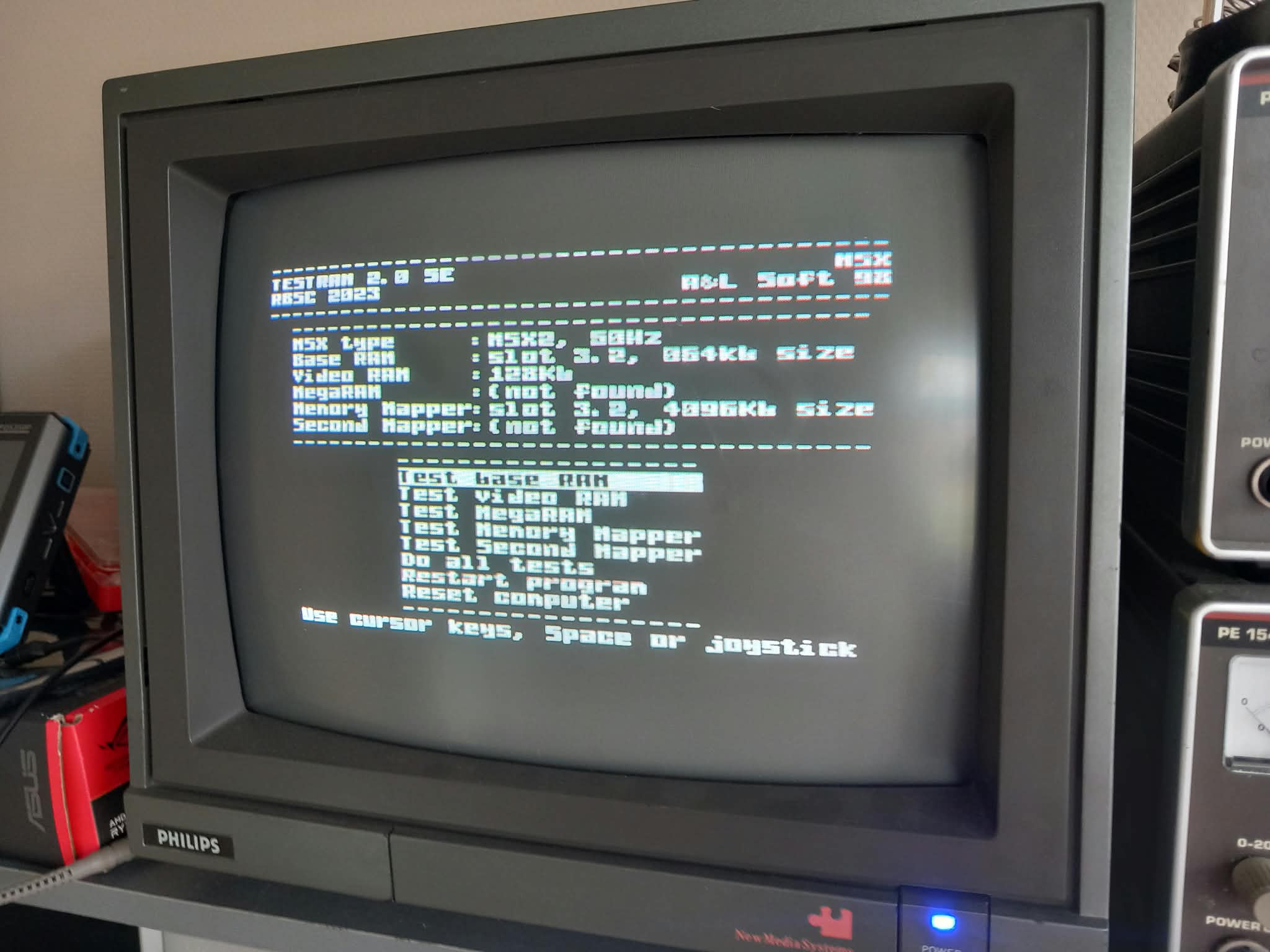
Plug in the finished PCB, carefully arranging the wires so they do not get trapped between the pin headers and DIP sockets. Power on the computer. With the stock ROM, the boot screen should report 128 KB of user RAM. Run a RAM checker to verify all 4096 KB.
The RAM is an HY5117404B, represented by the custom HYB5117400BJ symbol in the schematic. The custom 1464 symbol does not identify a manufacturer part number, so its exact component cannot be determined from the schematic alone.
| Qty | Value | Footprint | References |
|---|---|---|---|
| 11 | 100nf | Capacitor_SMD:C_0805_2012Metric | C1, C2, C131, C131B1, C131B2, C147, C147B1, C149, C149B1, C157B1, C180B1 |
| 3 | 74LS125 | Package_SO:SOIC-14_3.9x8.7mm_P1.27mm | IC131, IC131B1, IC131C1 |
| 2 | 74LS157 | Package_SO:SOIC-16_3.9x9.9mm_P1.27mm | IC147, IC147B1 |
| 2 | 74LS670 | Package_SO:SOIC-16_3.9x9.9mm_P1.27mm | IC149, IC149B1 |
| 2 | HY5117404B | custom_footprints:SOJ-2624_7.62x18.415mm_P1.27mm | U1, U2 |
| 2 | Pin Header 2x8 2,54mm Rounded | custom_footprints:PinHeader_2x08_P2.54mm_Vertical | CONN147, CONN149 |
| 2 | Pin Header 2x9 2,54mm Rounded | custom_footprints:PinHeader_2x09_P2.54mm_Vertical | CONN133, CONN134 |
| 1 | 74LS00 | Package_SO:SOIC-14_3.9x8.7mm_P1.27mm | IC180B1 |
| 1 | 74LS08 | Package_SO:SOIC-14_3.9x8.7mm_P1.27mm | IC157B1 |
| 1 | Conn_01x10_Pin | Connector_PinHeader_1.27mm:PinHeader_1x10_P1.27mm_Horizontal | J1 |
| 1 | Pin Header 2x7 2,54mm Rounded | custom_footprints:PinHeader_2x07_P2.54mm_Vertical | CONN131 |
iricryst/4mb-mapper-nms8280
A low-profile PCB implementation of the 4 MB memory mapper for the Philips NMS 8280 MSX2, based on the original design by Hans Oranje.

kev-ju/PC-Retro-MTM
Modern KiCad version of the IBM 5150 system board originally created by MTM Scientific, Inc.

Nakazoto/CenturionComputer
This is just a simple backup of all the files related to the Centurion that I have stored on my HD. The Wiki itself has far more in-depth information about the Centurion and it's individual cards.

Bambelweeny57/OSI-600D-SuperBoard-II
KiCad 10 recreation of the Ohio Scientific Superboard II Model 600 rev D (1980) with Cherry MX keyswitches, 27C16/2816 ROMs, full schematic and assembly guide.

frubem/NE_Delta_Schematics
Forked from https://codeberg.org/hkzlab/NE_Delta_Schematics

skiselev/zeta_sbc
Zeta SBC is an Zilog Z80 based single board computer. It is inspired by Ampro Little Board Z80 and N8VEM project. Zeta SBC is software compatible with RomWBW Firmware


tergav17/Z80-MegaMapper
Z80 interposer board providing extended memory and I/O instruction mapping

lynchaj/duodyne
Duodyne is a hobbyist retrocomputer system designed to run ROMWBW. It is comprised of modules on a system bus
It measures 102.2 × 68.2 mm and has 2 copper layers, 1.6 mm thick.
28 parts, built around the 74LS125DC, 74LS157PC, 74LS670 and 74LS00SC. The full list of its parts is on this page, with links to each part's symbol and footprint where PCBKit's library has them.
From the iricryst/4mb-mapper-nms8280 repository on GitHub, at the commit this page was made from: the board is kicad_alll_smd/4mb mapper nms8280.kicad_pcb and its schematic KICAD/4mb mapper nms8280.kicad_sch. PCBKit opens the board in the browser, with nothing to install.
Its repository states no licence, so its author keeps all rights: ask iricryst before reusing the design.