

2 layers279.4 × 203.2 mm
Z180GDC
lynchaj/rhyophyre
Single Board Computer featuring Zilog Z180 processor and NEC µPD7220 Graphics Display Controller
249 parts12

 skiselev/zeta_sbc53
Zeta SBC is an Zilog Z80 based single board computer. It is inspired by Ampro Little Board Z80 and N8VEM project. Zeta SBC is software compatible with RomWBW Firmware
Z80-SBC is an open-source printed circuit board by skiselev, from the skiselev/zeta_sbc repository on GitHub, published under the GPL-3.0 licence. It is a 2-layer board of 170.2 × 100 mm with 75 parts on 144 nets, routed with 2,861 tracks and 205 vias.
It is built around the 74LS125DC, MAX202ID and 74LS670, with the 74LS14PC, 74LS174DC and 74LS32SC among its other parts. Its parts include 26 capacitors, 22 ICs, 6 connectors, 4 resistors and 3 diodes. It belongs with the computers and single-board computers and retro computing and games boards of this library.


Zeta SBC V2 is a redesigned version of Zeta SBC. Compared to the first version this version features updated MMU with four banks, each one of those banks can be mapped to any 16 KiB page in 1 MiB on-board memory. It adds Z80 CTC which is used for generating periodic interrupts and as a vectored interrupt controller for UART and PPI. The FDC is replaced with 37C65. Compared to FDC9266 used in Zeta SBC it integrates input/output buffers and floppy disk control latch. Additionally 37C65 FDC is easier to obtain than FDC9266. And lastly it is made using CMOS technology and more power efficient than FDC9266
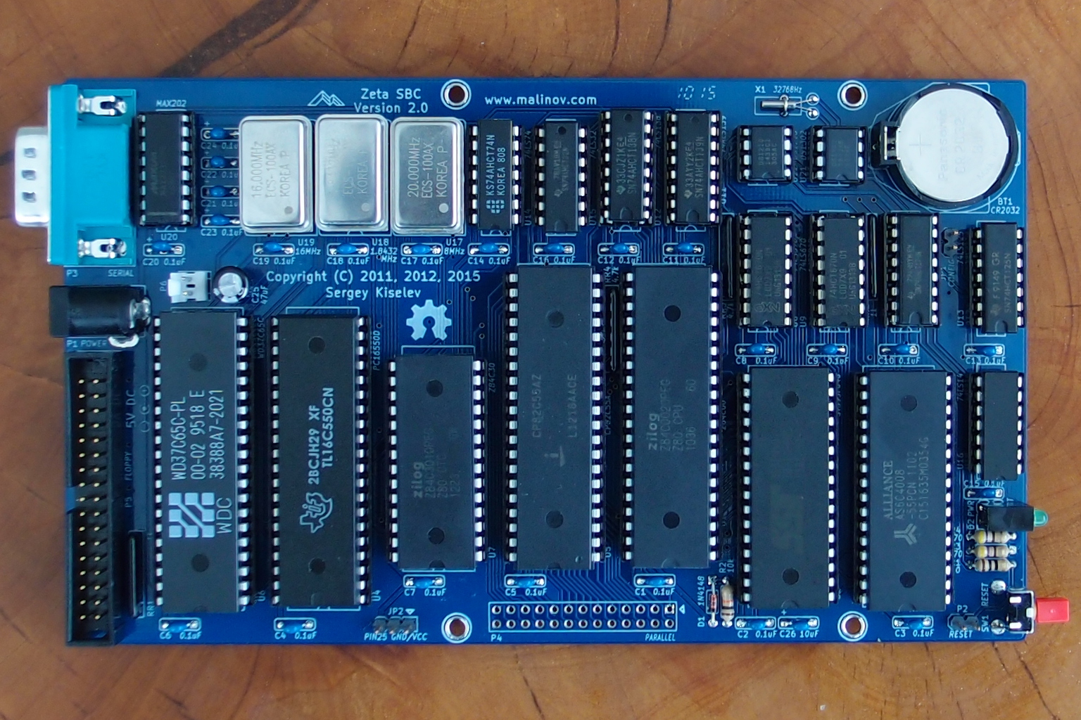
(FIXME: Picture shows Zeta SBC V1. Replace with Zeta SBC V2 when available.)
Zeta SBC V2 features following components:
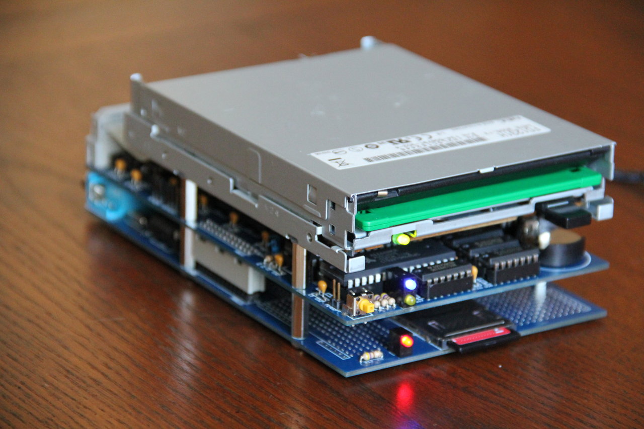
Zeta SBC V2 is compact and easy to build:
File downloads are at the bottom of this page.
Zeta SBC V2 - Schematic - Color - 2.0.pdf
Zeta SBC V2 - Board - Color - 2.0.pdf
Zeta SBC V2 - Gerber - 2.0.zip
Zeta SBC V2 features a 512 KiB Flash ROM, and 512 KiB SRAM. The Flash ROM is used for the boot loader, monitor, OS (CP/M and ZSDOS at this point), and ROM disk. The SRAM is battery-backed, and is used for applications and for a RAM disk.
The 64 KiB Z80 memory address space is divided into four 16 KiB memory banks:
The physical memory (512 KiB Flash ROM and 512 KiB SRAM) is divided into 16 KiB pages:
Page select registers are used to map physical memory pages to the banks in Z80 address space:
Following a power on or a hard reset the memory paging mechanism is disabled, and memory address lines MA19 - MA14 are pulled down. So that page #0 (ROM addresses 00000h to 03FFF) is mapped to all four banks. That page should contain a boot loader that (among other things) configures and enables memory paging. Once page select registers are configured properly the memory paging can be enabled by setting bit 1 of MPGENA (7Ch) register.
Zeta SBC V2 uses CTC as the source of vectored interrupts. For interrupts to function properly Z80 needs to be set to interrupt mode 2.
CTC can generate periodic interrupts by dividing CTC clock (921.6 kHz) using channels 0 and 1 configured in counter mode. The CTC clock is connected to the trigger input of channel 0, and the ZC (zero count) output of channel 0 is connected the trigger input of channel 1. So that channel 0 will divide the clock, and the resulting signal will be divided further using channel 1.
In this example channel 0 is programmed with time constant of 256, so it will divide the input clock by 256, resulting in 3.6 kHz pulses. The channel 1 is programmed with down counter of 240, and will divide 3.6 kHz clock by 240, resulting in 15 Hz signal. That channel is also programmed to generate an interrupt every time counter reaches 0.
01000111 to the channel 0. Configure the channel in the counter mode.00000000 to the channel 0. Set the time constant to 256.11000111 to the channel 1. Configure the channel in the counter mode and enable interrupt when counter reaches 0.11110000 to the channel 1. Set the time constant to 240, so that the interrupt will be generated every 1/15 of a second.VVVVV000 to the channel 0. Set bits 7-3 of the interrupt vector. Bits 15-8 are set to the value of I register, bits 2 and 1 are set to the CTC channel number that caused the interrupt. Bit 0 is always 0. Note that each interrupt vector takes 2 bytes of memory and it should start on an even address.CTC can be used as interrupt controller for UART and 8255 PPI using channels 2 and 3 respectively. In this case a CTC channel needs to be programmed for counter mode operation with time constant of 1. So that the first transition on CLK/TG input will result in counter going to 0 and CTC generating an interrupt.
110L0111 to the selected channel. This configures the channel in the counter mode with interrupts enabled. Bit 4 (L) sets the triggering edge: 0 - falling edge; 1 - rising edge.00000001 to the selected channel. This loads value 1 to the time constant, so that an interrupt will be generated after detecting the first edge on the trigger input.VVVVV000 to the channel 0. This sets bits 7-3 of the interrupt vector. Bits 15-8 are set to the I register, bits 2 and 1 are set to the CTC channel number that caused the interrupt. Bit 0 is always 0. Note that each interrupt vector takes 2 bytes of memory and it should start on an even address.Zeta SBC V2 includes a Maxim DS1302 RTC chip for timekeeping. It uses a CR2032 battery for power backup. The DS1302 has a 3-wire serial interface, and it is programmed through the RTC register (70h) using bit-banging. See Input/Output Ports section for the RTC register description. Please refer to DS1302 datasheet for programming information, and to the RomWBW (dsrtc.asm) for an RTC interface implementation.
JP1 is a software configuration jumper. It can be read by software using RTC port (70h) bit 6. This jumper is used by the RomWBW firmware with the ParPortProp support to configure the console device: it will use UART when this jumper is installed, and ParPortProp / VGA terminal when the jumper is not installed.
JP2 connects pin 25 of the parallel port P4 to either GND or Vcc (+5). Note that pin 1 is the pin that is closer to the parallel connector.
Warning: If JP2 is set incorrectly, it is possible to create a short circuit of the 5 Volt power supply.
| Jumper Position | Description |
|---|---|
| 1-2 | P4 pin 25 is connected to the ground |
| 2-3 | P4 pin 25 is connected to Vcc. Use this position with PPIDE, make sure to set jumper K1 on PPIDE to position 2-3. Please refer to PPIDE documentation for more information. |
| no jumper* | P4 pin 25 is left open |
* default
Connect regulated +5V power supply to this connector.
| Pin | Description |
|---|---|
| tip (the inner contact) | Positive terminal - +5V |
| barrel / sleeve | Negative terminal - ground |
P2 is a connector for an external reset button.
P3 is the serial port connector. It is normally used for connecting a console or terminal. P3 uses pinout similar to that of IBM AT serial port (with some signals missing). Use a null modem cable to connect to a PC.
| Pin Number | Signal Name | Description and Notes |
|---|---|---|
| 1 | DCD | Carrier Detect; Not used - Not connected on the SBC |
| 2 | RX | Receive Data; Input to SBC |
| 3 | TX | Transmit Data; Output from SBC |
| 4 | DTR | Data Terminal Ready;Not used - Not connected on the SBC |
| 5 | Signal Ground | Connected to the SBC GND signal |
| 6 | DSR | Data Set Ready;Not used - Not connected on the SBC |
| 7 | RTS | Request to Send; Output from SBC |
| 8 | CTS | Clear to Send; Input to SBC |
| 9 | RI | Ring Indicator;Not used - Not connected on the SBC |
| Shield | DE9 Shield | Connected to the SBC GND signal |
P4 is the parallel port connector. It is connected directly to the 8255 PPI and can be used for attaching, a ParPortProp board, an IDE hard disk using the PPIDE mini board, or for controlling external devices (e.g. printer, watering system), or for extending the SBC (e.g. connecting an LCD display and a keyboard). The pinout of P4 is the same as in other N8VEM boards (SBC V1, SBC V2, SBC-188).
| Pin Number | Description | Pin Number | Description | Pin Number | Description | Pin Number | Description |
|---|---|---|---|---|---|---|---|
| 1 | PC0 | 9 | PC4 | 17 | PB7 | 25 | GND or VCC (see JP2) |
| 2 | PA0 | 10 | PA4 | 18 | PB0 | 26 | GND |
| 3 | PC1 | 11 | PC5 | 19 | PB6 | ||
| 4 | PA1 | 12 | PA5 | 20 | PB1 | ||
| 5 | PC2 | 13 | PC6 | 21 | PB5 | ||
| 6 | PA2 | 14 | PA6 | 22 | PB2 | ||
| 7 | PC3 | 15 | PC7 | 23 | PB4 | ||
| 8 | PA3 | 16 | PA7 | 24 | PB3 |
P5 is the floppy interface connector. It uses PC compatible pinout. When using a PC floppy cable with a twist, Drive A (ID 0) is the drive after the twist and Drive B (ID 1) is the drive before the twist. When using only one FDD, either a twisted cable can be used, or the BIOS can be patched to use Drive B.
| Pin Number | Description | Direction (relative to the SBC) | Connected to |
|---|---|---|---|
| 1-33 | Odd pins are GND | GND | |
| 2 | High Density. This signal is ignored by most (all?) 3.5" drives. | Output | DOR (bit 6) |
| 4, 6 | Not used | No connection | |
| 8 | Index Pulse | Input | Schmidt Trigger, FDC (IDX) |
| 10 | Motor On B | Output | DOR (bit 1), Buffer |
| 12 | Drive Select A | Output | FDC (US0, US1), Decoder |
| 14 | Drive Select B | Output | FDC (US0, US1), Decoder |
| 16 | Motor On A | Output | DOR (bit 1), Buffer |
| 18 | Direction | Output | FDC (LCT/DIR), Multiplexer |
| 20 | Step | Output | FDC (FR/STEP), Multiplexer |
| 22 | Write Data | Output | FDC (WDOUT), OC Buffer |
| 24 | Write Enable | Output | FDC (WE), OC Buffer |
| 26 | Track Zero | Input | Multiplexer, FDC (FLT/TR0) |
| 28 | Write Protect | Input | Multiplexer, FDC (WP/TS) |
| 30 | Read Data | Input | Schmidt Trigger, FDC (~DSKD) |
| 32 | Select Head | Output | FDC (HD), OC Buffer |
| 34 | Disk Changed | Input | DIR (bit 0) |
P6 is the 5V power output for the floppy drive. Alternatively it can be used instead of P1 for supplying power to the board. It is recommended to use a polarized header for P6 to avoid incorrect power polarity which probably will destroy FDD or components on the SBC board.
| Pin Number | Description |
|---|---|
| 1 | 5V |
| 2 | GND |
Warning P6 connector's key is reversed compared to Zeta SBC V 1.x. Please pay attention when upgrading from older boards. The polarity marking on the silkscreen is correct.
Disclaimer: I did my best to make sure that components listed in this BOM will be compatible with Zeta SBC V2. Obviously I didn't order all of components listed here, and I was not able to actually verify that they will work. Please make sure to double check specifications on manufacturer's and seller's web site before ordering. Please let me know if you found any problems or incompatibilities.
Many components have multiple part numbers listed in BOM. There are some differences between various part numbers, such as:
If unsure what to order, read specifications on seller's and manufacturer's web sites. Also please read Replacement Notes below. Finally, consult people on N8VEM news group.
| Component type | Reference | Description | Quantity | Possible sources and notes |
|---|---|---|---|---|
| PCB | Zeta SBC V2 PCB Version 2.0 | 1 | Order from Sergey | |
| Battery Holder | BT1 | CR2032 batter holder, 20 mm lead spacing | 1 | Mouser 122-2420-GR,122-2620-GR;Jameco 355434 |
| Capacitor | C1 - C24 | 0.1 uF ceramic, 5.08 mm lead spacing | 24 | Mouser 810-FK28X7R1H104K,80-C323C104K5R; Jameco 25523 |
| Capacitor | C25 | 47 uF, 6.3 V electrolytic | 1 | Mouser 667-ECA-1HHG470;Jameco 31114 |
| Capacitor | C26 | 10 uF ceramic, 5.08 mm lead spacing | 1 | Mouser 810-FK24X5R1C106K Note: Can be replaced with tantalum or electrolytic capacitors |
| Diode | D1 | 1N4148 | 1 | Mouser 512-1N4148,771-1N4148-T/R;Jameco 36038,179215 |
| Diode | D2, D3 | Bi-level LED indicator | 1 | Mouser 696-SSF-LXH240GYD; Jameco: Search for uni-color bi-level LED |
| Standoff | HOLE1, HOLE2, HOLE3, HOLE4 | Standoff, M3 male / female, 20 mm | 4 | Mouser 534-24317,534-25505,855-R30-3012002 Note: The length of male end of these standoffs is 8 mm. It is too long for some floppy disk drives (you'll notice that standoff doesn't go completely inside the floppy drive mount hole). In this case cut a few millimeters using a file or a fine saw. |
| Screw | HOLE1, HOLE2, HOLE3, HOLE4 | Screw, M3, 6 mm | 4 | Use regular 3 mm floppy or CD-ROM drive mounting screws. Mouser 534-29311 |
| Connector | JP1, P2 | 2x1 pin header | 2 | Mouser 649-78229-102HLF;Jameco 108338 |
| Connector | JP2 | 3x1 pin header | 1 | Mouser 649-69190-103HLF,649-78229-103HLF;Jameco 109576 |
| Connector | P1 | DC jack | 1 | Mouser 806-KLDX-0202-A;Jameco 101178 |
| Connector | P3 | DE9M, right angle PCB mount | 1 | Mouser 806-K22X-E9P-N,806-K22X-E9P-N-99 (teal color),571-7478404;Jameco 104943,614459,614432; |
| Connector | P4 | 13x2 pin header | 1 | Mouser 649-68602-126HLF,649-77313-824-26LF;Jameco 53495 Note: don't use shrouded connector, as it will interfere with the standoff and other components. |
| Connector | P5 | 17x2 pin header shrouded | 1 | Mouser 517-30334-6002,571-1033087,571-5103308-7;Jameco 68583,753547 |
| Connector | P6 | 2 pin header with friction lock | 1 | Mouser 571-6404562,571-3-641126-2,571-3-641215-2;Jameco 232266,613931; Corresponding female connector: Mouser 571-770602-2;Jameco 234798Contacts (2 contacts needed):Mouser 571-770666-1;Jameco 234923,736501; It is recommended to use a polarized header to avoid incorrect power polarity. |
| Resistor | R1 | 10 Ohm, 1/4 W | 1 | Mouser 291-10-RC;Jameco 690380 |
| Resistor | R2 | 10 kOhm, 1/4 W | 1 | Mouser 291-10K-RC; Jameco 691104 |
| Resistor | R3, R4 | 470 Ohm, 1/4 W | 2 | Mouser 291-470-RC; Jameco 690785 |
| Resistor Array | RR1, RR2 | 1 kOhm, 6 pin, bussed resistor array | 2 | Mouser 264-1.0K-RC,652-4306R-1LF-1K Note: When using CMOS U11, RR2 can have a higher value, for example 4.7k. This will reduce the power consumption. |
| Resistor Array | RR3, RR4 | 4.7 kOhm, 6 pin, bussed resistor array | 2 | Mouser 264-4.7K-RC,652-4306R-1LF-4.7K |
| Switch | SW1 | Tactile switch, right angle | 1 | Mouser 653-B3F-3100,653-B3F-3152,706-95C06A2RAT,706-95C06C2RAT,706-95C06F2RATNote: Switches can have different actuator length. You might want to select the switch according your own preferences, for example the enclosure type you want to use, and whatever you want the reset button to stick out of the enclosure or to stay hidden inside. Jameco 1953575 |
| IC | U1 | Z80 CPU, CMOS, 40 pin DIP - Z84C00xxPEG | 1 | Mouser 692-Z84C0010PEG,692-Z84C0008PEG; Jameco 35705,35781 Frequency of U17 (CPU clock) oscillator should be less or equal to CPU frequency. 8MHz CPU recommended for 1.44 MB floppy disks support. |
| IC | U2 | 512 KiB flash, 32 pin DIP - 39SF040,29F040, 29C040 | 1 | Mouser 804-39SF0407CPHE; Jameco 242667 |
| IC | U3 | 512 KiB SRAM, 32 pin DIP -AS6C4008-55PCN | 1 | Mouser 913-AS6C4008-55PCN Note: Jameco 242448 and 157358 (BS62LV4006P) should work too, but they are way too expensive |
| IC | U4 | 16550 UART | 1 | Mouser 926-PC16550DN/NOPB; Jameco 288809 |
| IC | U5 | 8255 PPI | 1 | Mouser 968-CP82C55AZ,968-CP82C55A; Jameco 52417 Unicorn Electronics (order 82C55) |
| IC | U6 | FDC, 40 pin DIP WD37C65, FDC37C65, GM82C765 | 1 | Buy from eBay |
| IC | U7 | Z80 CTC, CMOS, 28 pin DIP -Z84C30xxPEG | 1 | Mouser 692-Z84C3010PEG,692-Z84C3008PEG; Jameco 35609 |
| IC | U8, U9 | 74LS670 | 2 | Mouser 595-SN74LS670N,771-HCT670N652; Jameco 47976 Unicorn Electronics 74LS670 |
| IC | U10 | 74LS174 | 1 | Mouser 595-SN74ALS174N,595-SN74LS174N,595-SN74AHCT174N; Unicorn Electronics; Jameco 46931 |
| IC | U11 | 74ALS139 | 1 | Mouser 595-SN74ALS139N,595-SN74LS139AN,595-CD74ACT139E,595-SN74AHCT139N; Unicorn Electronics; Jameco 46623,301268 |
| IC | U12 | 74LS138 | 1 | Mouser 595-SN74ALS138AN,595-SN74LS138N,595-SN74AHCT138N; Unicorn Electronics; Jameco 46607,301233,44927 |
| IC | U13 | 74LS125 | 1 | Mouser 595-SN74LS125AN,595-SN74AHCT125N; Unicorn Electronics; Jameco 46501 |
| IC | U14 | 74LS74 | 1 | Mouser 595-SN74ALS74AN,595-SN74AHCT74N; Jameco 48004,295726,45137 Unicorn Electronics 74ALS74, 74AHCT74 |
| IC | U15 | 74LS32 | 1 | Mouser 595-SN74ALS32N,595-SN74LS32N,595-SN74ACT32N,595-CD74ACT32E; Unicorn Electronics; Jameco 47466,295515 |
| IC | U16 | 74LS14 | 1 | Mouser 595-SN74LS14N,595-SN74AHCT14N; Unicorn Electronics; Jameco 46640,295460,44935 |
| IC | U17 | CPU clock oscillator, full can | 1 | See frequency selection note for U1. 4 MHz: Mouser 815-ACO-4-EK,520-TCF400-X;Jameco 27967 6 MHz: Mouser 520-TCF600-X 8 MHz: Mouser 815-ACO-8-EK,520-TCF800-X;Jameco 27991 10 MHz: Mouser 815-ACO-10-EK,520-TCF1000-X;Jameco 27887 20 MHz: Mouser 815-ACO-20-EK,520-TCF2000-X;Jameco 27932 |
| IC | U18 | 1.8432 MHz oscillator, full can | 1 | Mouser 520-TCF184-X; Jameco 27879 |
| IC | U19 | 16 MHz oscillator, full can | 1 | Mouser 520-TCF1600-X,815-ACO-16-EK |
| IC | U20 | MAX202 | 1 | Mouser 595-TRS202ECN,701-SP202ECP-L,700-MAX202CPE,700-MAX232ACP; Jameco 1800552,142535 |
| IC | U21 | DS1302 | 1 | Mouser 700-DS1302,700-DS1302N; Jameco 176778,780481 |
| IC | U22 | DS1210 | 1 | Mouser 700-DS1210; Jameco 114198 |
| IC Socket | U1, U4 - U6 | 40 pin 600 mil DIP socket | 4 | Mouser 517-4840-6000-CP,649-DILB40P223TLF;Jameco 41111 |
| IC Socket | U2, U3 | 32 pin 600 mil DIP socket | 2 | Mouser 517-4832-6000-CP,649-DILB32P223TL;Jameco 112301 |
| IC Socket | U7 | 28 pin 600 mil DIP socket | 1 | Mouser 517-4828-6000-CP,649-DILB28P223TLF |
| IC Socket | U8 - U12, U24 | 16 pin 300 mil DIP socket | 6 | Mouser 517-4816-3000-CP,649-DILB16P-223TLF;Jameco 37373 |
| IC Socket | U13 - U16 | 14 pin 300 mil DIP socket | 4 | Mouser 517-4814-3000-CP,649-DILB14P-223TLF;Jameco 37162 |
| IC Socket | U21, U22 | 8 pin 300 mil DIP socket | 2 | Mouser 517-4808-3000-CP,649-DILB8P223TLF;Jameco 51571 |
| Oscillator Socket | U17 - U19 | 4 pin 300 mil DIP full can oscillator socket | 3 | Mouser 535-1107741;Jameco 133006 |
| Crystal | X1 | 32768 Hz crystal | 1 | Mouser 695-CFS206-327KB-U,520-ECS327-6-13-X,628-VT200F-6PF20PPM;Jameco 14584 |
Zeta SBC V2 requires a regulated 5V power supply. Make sure that the tip of the power supply is the positive lead. System's power consumption varies depending on components used on SBC (CMOS CPU/PPI/UART vs. NMOS components, CMOS logic vs. TTL/LS vs. TTL/ALS) and CPU clock frequency. Also floppy disk drives are relatively power hungry (about 1 A max). Jameco carries quite a few regulated switching 5V wall adapters with different amperage. See these catalog pages:
http://www.jameco.com/Jameco/catalogs/c113/P105.pdf
http://www.jameco.com/Jameco/catalogs/c113/P106.pdf
Alternatively it is possible to use a linear power supply with 7805 or similar voltage regulator (make sure to use a heatsink, especially if powering a floppy drive).
Mods described here were intentionally not implemented on PCB to keep it simple.
| Link | Modified |
|---|---|
| Zeta SBC V2 - Assembled Board.JPG (853k) | Sergey Kiselev, Mar 30, 2015, 9:11 AM |
| Zeta SBC V2 - Board - Color - 2.0.pdf (1200k) | Sergey Kiselev, Jun 15, 2015, 10:48 AM |
| Zeta SBC V2 - Gerber - 2.0.zip (260k) | Sergey Kiselev, Jun 15, 2015, 10:47 AM |
| Zeta SBC V2 - KiCad - 2.0.zip (457k) | Sergey Kiselev, Jun 15, 2015, 10:47 AM |
| Zeta SBC V2 - Schematic - Color - 2.0.pdf (210k) | Sergey Kiselev, Jun 15, 2015, 10:48 AM |
| Zeta with ParPortProp - Perspective View.jpg (190k) | Sergey Kiselev, Jan 23, 2015, 11:40 AM |
| Qty | Value | Footprint | References |
|---|---|---|---|
| 19 | 0.1uF | Cap_Cer_508 | C1, C2, C3, C4, C5, C6, C10, C11, C12, C13, C14, C15, C16, C17, C18, C19 +3 |
| 5 | 0.1uF | Cap_Pol_508_3 | C20, C21, C22, C23, C24 |
| 4 | CONN_1 | HOLE_3MM | HOLE1, HOLE2, HOLE3, HOLE4 |
| 2 | 1k | Conn_SIL6 | RR1, RR2 |
| 2 | 4.7k | Conn_SIL6 | RR3, RR4 |
| 2 | 470 | Res_762 | R3, R4 |
| 2 | 74LS670 | IC_DIP16_300 | U8, U9 |
| 1 | 1.8432 | OSC_Full_Half_Can_DIP14 | U18 |
| 1 | 10 | Res_762 | R1 |
| 1 | 10k | Res_762 | R2 |
| 1 | 10uF | Cap_Pol_508_3 | C26 |
| 1 | 16MHz | OSC_Full_Half_Can_DIP14 | U19 |
| 1 | 1N4148 | Diode_762 | D1 |
| 1 | 32768Hz | CRYSTAL32768 | X1 |
| 1 | 47uF | Cap_Elec_Radial_5mm | C25 |
| 1 | 5V | Conn_Friction_Lock_2P_2.54mm | P6 |
| 1 | 74ALS139 | IC_DIP16_300 | U11 |
| 1 | 74LS125 | IC_DIP14_300 | U13 |
| 1 | 74LS138 | IC_DIP16_300 | U12 |
| 1 | 74LS14 | IC_DIP14_300 | U16 |
| 1 | 74LS174 | IC_DIP16_300 | U10 |
| 1 | 74LS32 | IC_DIP14_300 | U15 |
| 1 | 74LS74 | IC_DIP14_300 | U14 |
| 1 | 8MHz | OSC_Full_Half_Can_DIP14 | U17 |
| 1 | AS6C4008 | IC_DIP32_600 | U3 |
| 1 | CONFIG | Conn_Pin_Header_2x1_2.54mm_NoKey | JP1 |
| 1 | CP82C55A | IC_DIP40_600 | U5 |
| 1 | CR2032 | Battery_Holder_CR2032_Universal | BT1 |
| 1 | DS1210 | IC_DIP8_300 | U22 |
| 1 | DS1302 | IC_DIP8_300 | U21 |
| 1 | FLOPPY | Conn_Pin_Header_17x2_2.54mm_Shrouded | P5 |
| 1 | HALT | Conn_Pin_Header_2x1_2.54mm | D3 |
| 1 | MAX202 | IC_DIP16_300 | U20 |
| 1 | OSHW-logo_silkscreen-front_8mm | OSHW-logo_silkscreen-front_8mm | G*** |
| 1 | PARALLEL | pin_array_13x2 | P4 |
| 1 | PC16550D | IC_DIP40_600 | U4 |
| 1 | PIN25 GND/VCC | Conn_Pin_Header_3x1_2.54mm | JP2 |
| 1 | POWER | Conn_Power_Jack | P1 |
| 1 | PWR | Conn_Pin_Header_2x1_2.54mm | D2 |
| 1 | RESET | Conn_Pin_Header_2x1_2.54mm_NoKey | P2 |
| 1 | RESET | Switch_Tactile_6mm_Right | SW1 |
| 1 | SERIAL | Conn_Dsub_DE9M | P3 |
| 1 | ST39SF040 | IC_DIP32_600 | U2 |
| 1 | WD37C65C | IC_DIP40_600 | U6 |
| 1 | Z84C00 | IC_DIP40_600 | U1 |
| 1 | Z84C30 | IC_DIP28_600 | U7 |
lynchaj/rhyophyre
Single Board Computer featuring Zilog Z180 processor and NEC µPD7220 Graphics Display Controller


kev-ju/PC-Retro-MTM
Modern KiCad version of the IBM 5150 system board originally created by MTM Scientific, Inc.

Bambelweeny57/OSI-600D-SuperBoard-II
KiCad 10 recreation of the Ohio Scientific Superboard II Model 600 rev D (1980) with Cherry MX keyswitches, 27C16/2816 ROMs, full schematic and assembly guide.


RichCini/LomasBoards
Small repository of files/data related to Lomas Data Products S-100 boards.
It measures 170.2 × 100 mm and has 2 copper layers, 1.6 mm thick.
75 parts, built around the 74LS125DC, MAX202ID, 74LS670 and 74LS14PC. The full list of its parts is on this page, with links to each part's symbol and footprint where PCBKit's library has them.
From the skiselev/zeta_sbc repository on GitHub, at the commit this page was made from: the board is KiCad/Z80-SBC.kicad_pcb. PCBKit opens the board in the browser, with nothing to install.
Its repository publishes it under the GPL-3.0 licence: you may reuse it on that licence's terms (keep the author's notice, and for a copyleft licence share your changes alike).