2 layers48 × 40 mm

 imad-drs/mini_encabulator_PCB3
A complete PCB design exercise demonstrating schematic capture, component selection, and board layout using KiCAD. This project implements a simple LED blinker with user-controllable blink rate.
Encabulator is an open-source printed circuit board by imad-drs, from the imad-drs/mini_encabulator_PCB repository on GitHub. It is a 2-layer board of 55.2 × 43.8 mm with 17 parts on 12 nets, routed with 67 tracks and 2 vias.
It is built around the ATTINY85-20SU, LM1117MP-5.0 and MBR0520. Its parts include 4 connectors, 3 resistors, 2 capacitors, 2 ICs and 1 diode. It belongs with the AVR (ATmega, ATtiny) boards of this library.


A complete PCB design exercise demonstrating schematic capture, component selection, and board layout using KiCAD. This project implements a simple LED blinker with user-controllable blink rate.
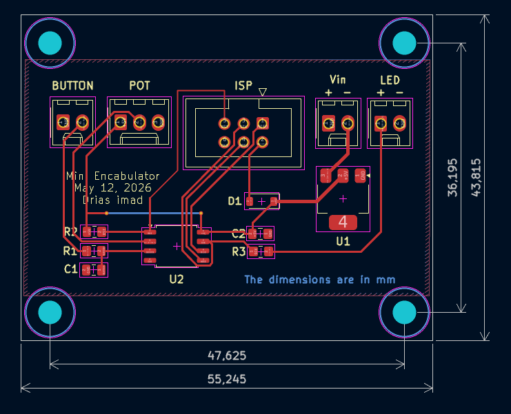 Final PCB layout with component placement and routing
The Mini Encabulator is a microcontroller-based device that:
This project was designed as a learning exercise for PCB design fundamentals, including proper power delivery, signal conditioning, and mechanical integration with an enclosure.
| Component | Part Number | Package | Purpose | Quantity |
|---|---|---|---|---|
| Microcontroller | ATTiny85-20S | SOIC-8 | Main processor | 1 |
| Voltage Regulator | LM1117MP-5.0 | SOT-223 | 5V power supply | 1 |
| Protection Diode | MBR0520 | SOD-123 | Reverse current protection | 1 |
| Component | Value | Package | Purpose | Quantity |
|---|---|---|---|---|
| Resistor | 10kΩ | 0805 | RESET pull-up | 1 |
| Resistor | 10kΩ | 0805 | Button debounce | 1 |
| Resistor | 1kΩ | 0805 | LED current limit | 1 |
| Capacitor | 1µF | 0805 | Power decoupling | 1 |
| Capacitor | 1µF | 0805 | Button debounce | 1 |
| Connector | Type | Pitch | Purpose | Quantity |
|---|---|---|---|---|
| Power Input | Molex KK-254 2-pin | 2.54mm | External power | 1 |
| Button | Molex KK-254 2-pin | 2.54mm | User input | 1 |
| LED | Molex KK-254 2-pin | 2.54mm | Indicator output | 1 |
| Potentiometer | Molex KK-254 3-pin | 2.54mm | Analog input | 1 |
| ISP Header | IDC 2x3 | 2.54mm | Programming interface | 1 |
| Pin | Function | Connected To |
|---|---|---|
| 1 (PB5) | RESET | Pull-up resistor, ISP header |
| 2 (PB3) | Potentiometer | J5 (POT wiper) |
| 3 (PB4) | Button Input | J3 (BUTTON) through RC filter |
| 4 (GND) | Ground | Ground plane |
| 5 (PB0) | MOSI/LED | R4 → J4 (LED) |
| 6 (PB1) | MISO | ISP header |
| 7 (PB2) | SCK | ISP header |
| 8 (VCC) | Power | +5V rail, C1 decoupling |
J1 (Button): Momentary Switch
J3 (Vin): Power Input
J4 (LED): Indicator LED
J5 (Pot): Potentiometer (10kΩ recommended)
Contributions are welcome! Please feel free to submit issues or pull requests.
Drias Imad Eddine - drias.imad2006@gmail.com
⭐ If you found this project helpful, please consider giving it a star!
| Qty | Value | Footprint | References |
|---|---|---|---|
| 4 | MountingHole | MountingHole:MountingHole_3.2mm_M3 | H1, H2, H3, H4 |
| 2 | 10k | Resistor_SMD:R_0805_2012Metric_Pad1.20x1.40mm_HandSolder | R1, R2 |
| 2 | 1u | Capacitor_SMD:C_0805_2012Metric_Pad1.18x1.45mm_HandSolder | C1, C2 |
| 1 | 1k | Resistor_SMD:R_0805_2012Metric_Pad1.20x1.40mm_HandSolder | R3 |
| 1 | ATtiny85-20S | Package_SO:SOIC-8_5.3x5.3mm_P1.27mm | U2 |
| 1 | AVR-ISP-6 | Connector_IDC:IDC-Header_2x03_P2.54mm_Vertical | ISP |
| 1 | BUTTON | Connector_Molex:Molex_KK-254_AE-6410-02A_1x02_P2.54mm_Vertical | J1 |
| 1 | LED | Connector_Molex:Molex_KK-254_AE-6410-02A_1x02_P2.54mm_Vertical | J4 |
| 1 | LM1117MP-5.0 | Package_TO_SOT_SMD:SOT-223 | U1 |
| 1 | MBR0520 | Diode_SMD:D_SOD-123 | D1 |
| 1 | POT | Connector_Molex:Molex_KK-254_AE-6410-03A_1x03_P2.54mm_Vertical | J5 |
| 1 | Vin | Connector_Molex:Molex_KK-254_AE-6410-02A_1x02_P2.54mm_Vertical | J3 |

anandpraj/Mini-Encabulator-PCB-Design
This simple device only does two things: ● Blinks an LED when the user holds down a button. ● Sets blink rate proportional to potentiometer position.


NYDEREK/LineFollower_GRUZIK2.0-light
GRUZIK2.0 is simple light construction made for "line follower light" competition

SherpaModular/RawWaves
Raw Waves is a eurorack synthesizer module that plays RAW or WAV sample files from a micro SDcard. It is a derivate work of "Radio Music" from Tom Whitwell. Raw Waves is released under a CC-by-SA 3.0 license.

aNThiCu/AirsoftETU
The code for a airsoft MOSFET board that includes the trigger , active break mode and semi-auto,full-auto detection.

adarwoo/modbus_relay
A modbus RTU relay board with 3 relays for the CNC. This uses the ASX framework

chithigun23/ANUFS-BSPD-2026
ANUFS's BSPD for 2026 Formula SAE ICE Car. The goal of this project is to be AEC-Q100/Q101/Q200 compliant.
It measures 55.2 × 43.8 mm and has 2 copper layers, 1.6 mm thick.
17 parts, built around the ATTINY85-20SU, LM1117MP-5.0 and MBR0520. The full list of its parts is on this page, with links to each part's symbol and footprint where PCBKit's library has them.
From the imad-drs/mini_encabulator_PCB repository on GitHub, at the commit this page was made from: the board is Encabulator.kicad_pcb and its schematic Encabulator.kicad_sch. PCBKit opens the board in the browser, with nothing to install.
Its repository states no licence, so its author keeps all rights: ask imad-drs before reusing the design.