Skip to the content
PCBKitNew board
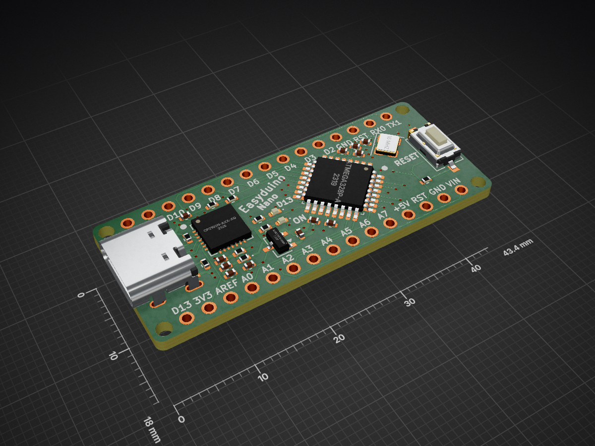
4 layers43.4 × 18 mmEasyduino Atmega Nano, the printed circuit board in 3D

Easyduino Atmega Nano

Hanqaqa/Easyduino755

Easily dive into different PCB KiCad designs of the most popular microcontroller devboards

Size
43.4 × 18 mm
Copper layers
4
Thickness
1.6 mm
Parts
31
Nets
62
Pads
187
Tracks, vias
332, 57
Pours
3
Routed
Yes
KiCad
KiCad 10.0 (file 20260206)
Created
13 Apr 2026
Updated
28 Jun 2026

Overview

Easyduino Atmega Nano is an open-source printed circuit board by Hanqaqa, from the Hanqaqa/Easyduino repository on GitHub, published under the CERN-OHL-P-2.0 licence. It is a 4-layer board of 43.4 × 18 mm with 31 parts on 62 nets, routed with 332 tracks and 57 vias.

It is built around the ATMEGA328P-AU and XC6206P502MR. Its parts include 12 capacitors, 7 resistors, 3 ICs, 3 diodes and 2 connectors. It belongs with the microcontroller boards boards and the ESP32, RP2040, STM32 and AVR (ATmega, ATtiny) boards of this library.

Main components

2

README

ESP32/readme.md

ESP32

The most popular WiFi Microcontroller

Schematic

KiCad Schematic symbols, footprints and 3D Models were obtained from their KiCad Github repository

Gerbers

Specs

  • Input Voltage: 5V-15V(External Source 5V Pin) 5V (USB) or 3.3V (3.3V Pin). ONLY USE ONE VOLTAGE INPUT AT A TIME
  • Output Current at 3.3V : 1 A (External Source) 500mA (USB)
  • No Polarity Protection (External Source)
  • Overcurrent Protection: None

References

ESP32 WROOM 32E

Decoupling capacitors
  • ESP32 Wroom 32 E datasheet p24 -> 3.3V pin needs one 22uF and one 100nF capacitors
Enable pin (EN)
  • ESP32 Devkit sch -> EN pin 10k resistor and 100nF capacitor
Thermal Pad
  • ESP32 Wroom 32 E datasheet p26 -> GND Thermal needs vias between pads. Needed vias are too small for my manufacturer. I will use bigger vias
Automatic Bootloader
  • ESP32 Devkit sch -> Automatic Bootloader.

USB-C

Filtering
  • USB Hardware Design Guidelines for FTDI ICs p8 -> 10nF Cap + Ferrite Bead + 100nF Cap + 4.7uF Cap
  • I disregarded such heavy filtering for the easier to implement 1uF and 100nF cap given in the CP2102 datasheet
  • I added a polyfuse with Ihold=500mA and Itrip=1A.
Differential Pair
  • USB needs 90 Ohm differential traces.
  • According to JLCPCB impedance calculator, with a JLC7628 prepreg and 6mil (0.15mm) space between lines
  • I have to use 9 mil tracks -> 0.2 mm
  • I will use a very short trace for D+ D- (around 2mm)
  • I have to place vias because of the pinout of USB C and CP2102. Some other people have done it with no problems
CP2102
  • CP2102 datasheet p15 -> VBUS will be tied to REGIN. 1uF and 100 nF will be added.
  • CP2102 datasheet p15 -> ESD Supression Diode for all three inputs of USB
  • CP2102 datasheet p15 and p19 -> 100nF for VDD output, 4.7 uF is optional for higher current circuits.
  • CP2102 datasheet p23 -> The VDD or 3.3 output can only provide 100mA. I will not use this as a voltage provider for the ciruit. I will use the AMS1117-3.3
  • CP2102 datasheet p15 -> RST pulled up via 4.7k and SUSPEND~ pulled down via 10k.
AMS1117-3.3V
  • AMS1117 Datasheet p1 -> 3.3V/1A Output with 5-15V Input
  • AMS1117 Datasheet p4 -> 22uF tantalum capacitor on input and output.

KiCad Render

Parts

31
QtyValueFootprintReferences
7100nCapacitor_SMD:C_0402_1005MetricC2, C3, C4, C5, C6, C7, C8
45.1kResistor_SMD:R_0402_1005MetricR1, R2, R3, R4
31uCapacitor_SMD:C_0402_1005MetricC1, C11, C12
222pCapacitor_SMD:C_0402_1005MetricC9, C10
22kResistor_SMD:R_0402_1005MetricR6, R7
2LEDLED_SMD:LED_0402_1005MetricD1, D3
116 MHzCrystal:Crystal_SMD_3225-4Pin_3.2x2.5mmY1
1330Resistor_SMD:R_0402_1005MetricR5
1ATmega328P-APackage_QFP:TQFP-32_7x7mm_P0.8mmU1
1Arduino_Nano_v3.xModule:Arduino_Nano_WithMountingHolesA1
1CP2102N-Axx-xQFN28Package_DFN_QFN:QFN-28-1EP_5x5mm_P0.5mm_EP3.35x3.35mmU3
1D_SchottkyDiode_SMD:D_0402_1005MetricD2
1ICSPConnector_PinHeader_2.54mm:PinHeader_2x03_P2.54mm_VerticalJ2
1PolyfuseFuse:Fuse_0402_1005MetricF1
1SW_PushButton_Switch_SMD:SW_Tactile_SPST_NO_Straight_CK_PTS636Sx25SMTRLFSSW1
1USB_C_Receptacle_USB2.0Connector_USB:USB_C_Receptacle_G-Switch_GT-USB-7010ASVJ1
1XC6206P502MRPackage_TO_SOT_SMD:SOT-23-3U2

Questions

How big is the Easyduino Atmega Nano PCB?

It measures 43.4 × 18 mm and has 4 copper layers, 1.6 mm thick.

What parts does the Easyduino Atmega Nano use?

31 parts, built around the ATMEGA328P-AU and XC6206P502MR. The full list of its parts is on this page, with links to each part's symbol and footprint where PCBKit's library has them.

Where can I download the Easyduino Atmega Nano KiCad files?

From the Hanqaqa/Easyduino repository on GitHub, at the commit this page was made from: the board is Atmega328p Arduino Nano/Easyduino_Atmega_Nano.kicad_pcb and its schematic Atmega328p Arduino Nano/Easyduino_Atmega_Nano.kicad_sch. PCBKit opens the board in the browser, with nothing to install.

Can I use the Easyduino Atmega Nano design in my own project?

Its repository publishes it under the CERN-OHL-P-2.0 licence: you may reuse it on that licence's terms (keep the author's notice, and for a copyleft licence share your changes alike).

More from Hanqaqa/Easyduino

5
  • 4 layers21 × 51 mmEasyduino RP2040, the printed circuit board in 3D

    Easyduino RP2040

    Hanqaqa/Easyduino

    Easily dive into different PCB KiCad designs of the most popular microcontroller devboards

    65 parts755CERN-OHL-P-2.0
  • 4 layers68.8 × 53.6 mmEasyduino Atmega, the printed circuit board in 3D

    Easyduino Atmega

    Hanqaqa/Easyduino

    Easily dive into different PCB KiCad designs of the most popular microcontroller devboards
    38 parts755CERN-OHL-P-2.0
  • 4 layers25.9 × 63.9 mmEasyduino ESP32S3, the printed circuit board in 3D

    Easyduino ESP32S3

    Hanqaqa/Easyduino

    Easily dive into different PCB KiCad designs of the most popular microcontroller devboards

    35 parts755CERN-OHL-P-2.0
  • 4 layers23 × 53 mmEasyduino STM32F103, the printed circuit board in 3D

    Easyduino STM32F103

    Hanqaqa/Easyduino

    Easily dive into different PCB KiCad designs of the most popular microcontroller devboards

    30 parts755CERN-OHL-P-2.0
  • 4 layers28.4 × 47.9 mmEasyduino ESP32, the printed circuit board in 3D

    Easyduino ESP32

    Hanqaqa/Easyduino

    Easily dive into different PCB KiCad designs of the most popular microcontroller devboards

    29 parts755CERN-OHL-P-2.0

Similar boards

  • 4 layers43.4 × 18 mmNanoFlux EdgeCore, the printed circuit board in 3D

    NanoFlux EdgeCore

    MAHESH-THILAK-K/ADDITIONAL-PROJECT

    32 parts1Apache-2.0
  • 4 layers48 × 73 mmGrinder, the printed circuit board in 3D

    Grinder

    magnusnordlander/fifty-fifty

    A grinder controller for my Mazzer Major

    31 parts7MIT
  • 2 layers50 × 45 mmLightingBoard, the printed circuit board in 3D

    LightingBoard

    Champers5000/FauxLightWindow

    70 parts
  • 2 layers48.3 × 31.8 mmCosmonode ext02, the printed circuit board in 3D

    Cosmonode ext02

    exostic/Cosmonode_PCBs

    Kicad plans to design a base node as the main PCB. It also contains extensions adapted for different set of sensors/connectors.

    24 parts
  • 2 layers48.3 × 31.8 mmCosmonode ext02, the printed circuit board in 3D

    Cosmonode ext02

    getlarge/Cosmonode_PCBs

    Kicad plans to design a base node, also contains extensions adapted for different set of sensors/connectors.

    23 parts1
  • 2 layers50.5 × 128.5 mmOpenThereminV45, the printed circuit board in 3D

    OpenThereminV45

    GaudiLabs/OpenThereminV4

    Open Source Theremin Instrument

    107 parts249GPL-3.0
  • 2 layers152 × 88 mmRFBitBangSMT, the printed circuit board in 3D

    RFBitBangSMT

    profdc9/RFBitBanger

    A QRP digital transceiver created from readily available parts for off-the-grid maintenance

    271 parts222