
2 layers319.7 × 58.4 mm
 Gregification/BeeMS5
Battery Management System
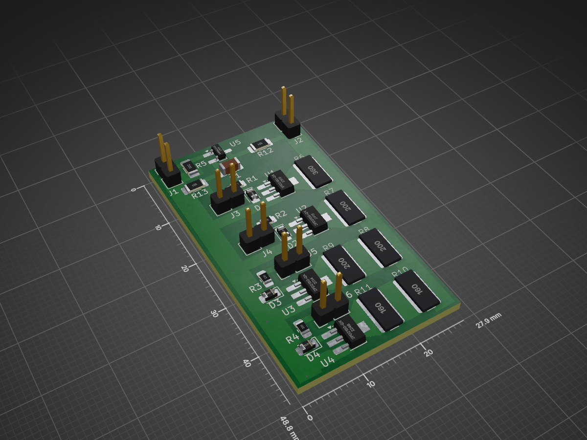
Cell Balancing testing is an open-source printed circuit board by Gregification, from the Gregification/BeeMS repository on GitHub, published under the MIT licence. It is a 2-layer board of 27.9 × 48.8 mm with 29 parts on 19 nets, routed with 53 tracks and 4 vias.
It is built around the DMN62D0U and TS4148. Its parts include 13 resistors, 6 connectors, 5 ICs, 4 diodes and 1 capacitor. It belongs with the power boards of this library.
Battery Management System (BMS)
a work in progress
BMS for University Of Texas At Arlington's FSAE Race team's E27 vehicle.
point of contact for this repo is George Boone
| Qty | Value | Footprint | References |
|---|---|---|---|
| 4 | 226 | Resistor_SMD:R_0805_2012Metric_Pad1.20x1.40mm_HandSolder | R1, R2, R3, R4 |
| 4 | 2PD2150-QX | Package_TO_SOT_SMD:SOT-89-3_Handsoldering | U1, U2, U3, U4 |
| 4 | TS4148 | Diode_SMD:D_0805_2012Metric_Pad1.15x1.40mm_HandSolder | D1, D2, D3, D4 |
| 4 | ~ | Connector_PinHeader_2.54mm:PinHeader_1x02_P2.54mm_Vertical | J3, J4, J5, J6 |
| 3 | 20 | zzLocalLibraries-Footprints:imperial wide resistor R_ 3264 | R7, R8, R9 |
| 2 | 100 | Resistor_SMD:R_1206_3216Metric_Pad1.30x1.75mm_HandSolder | R12, R13 |
| 2 | 16 | zzLocalLibraries-Footprints:imperial wide resistor R_ 3264 | R10, R11 |
| 1 | 100n | Capacitor_SMD:C_1206_3216Metric_Pad1.33x1.80mm_HandSolder | C1 |
| 1 | 36 | zzLocalLibraries-Footprints:imperial wide resistor R_ 3264 | R6 |
| 1 | 4.99k | Resistor_SMD:R_1206_3216Metric_Pad1.30x1.75mm_HandSolder | R5 |
| 1 | DMN62D0U | Package_TO_SOT_SMD:SOT-23_Handsoldering | U5 |
| 1 | cell | Connector_PinHeader_2.54mm:PinHeader_1x02_P2.54mm_Vertical | J2 |
| 1 | pwm | Connector_PinHeader_2.54mm:PinHeader_1x02_P2.54mm_Vertical | J1 |
It measures 27.9 × 48.8 mm and has 2 copper layers, 1.6 mm thick.
29 parts, built around the DMN62D0U and TS4148. The full list of its parts is on this page, with links to each part's symbol and footprint where PCBKit's library has them.
From the Gregification/BeeMS repository on GitHub, at the commit this page was made from: the board is hardware/Cell Balancing testing/Cell Balancing testing.kicad_pcb and its schematic hardware/CAN DC SS switch/CAN DC SS switch.kicad_sch. PCBKit opens the board in the browser, with nothing to install.
Its repository publishes it under the MIT licence: you may reuse it on that licence's terms (keep the author's notice, and for a copyleft licence share your changes alike).


peterisza/iec62386-wall-panel
Wall panel for smart homes. 2 wires, no polarity, arbitrary bus topology, exchangeable front panel with hardware capacitive buttons, temperature+humidity+pressure+CO2.

myriadrf/reference-development-kit
The Myriad-RF Reference Hardware design files and firmware

myriadrf/STREAM
FPGA development platform for high-performance RF and digital design


jaredhumphreys3141/MECHANICAL-NUMPAD-PCB
This is a custom numeric pad that is designed to be usable on the right side of the keyboard or on the left (With a mirrored layout if required). There is a gap in the top row and the second row of 1.25U.