2 layers78 × 622 mm
 leventelist/audio_interface
Audio interface
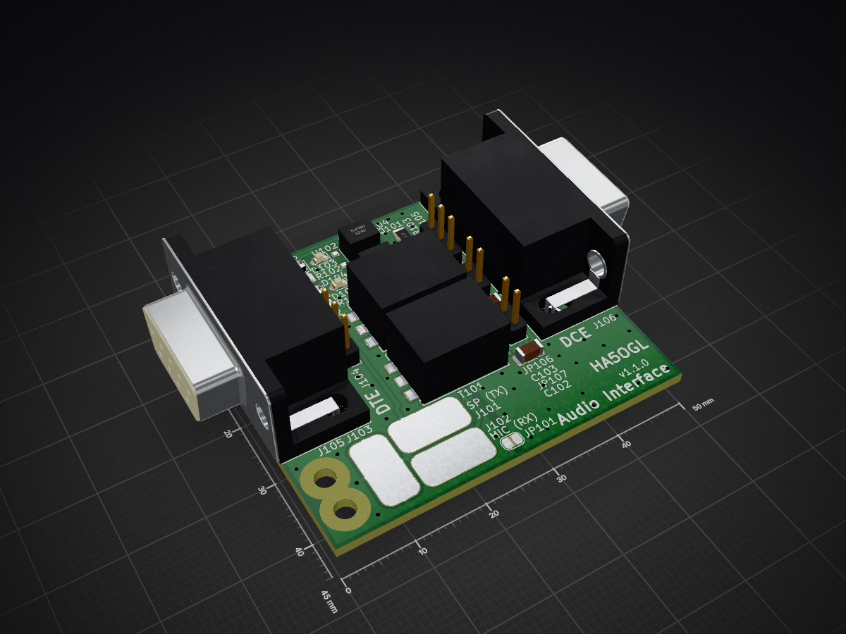
Audio interface is an open-source printed circuit board by leventelist, from the leventelist/audio_interface repository on GitHub. It is a 2-layer board of 50 × 45 mm with 31 parts on 26 nets, routed with 140 tracks and 114 vias.
It is built around the TLP185, BC847C and SM-LP-5001, with the TS4148 among its other parts. Its parts include 6 connectors, 4 diodes, 3 capacitors, 3 resistors and 2 ICs. It belongs with the audio and music and interfaces and adapters boards of this library.


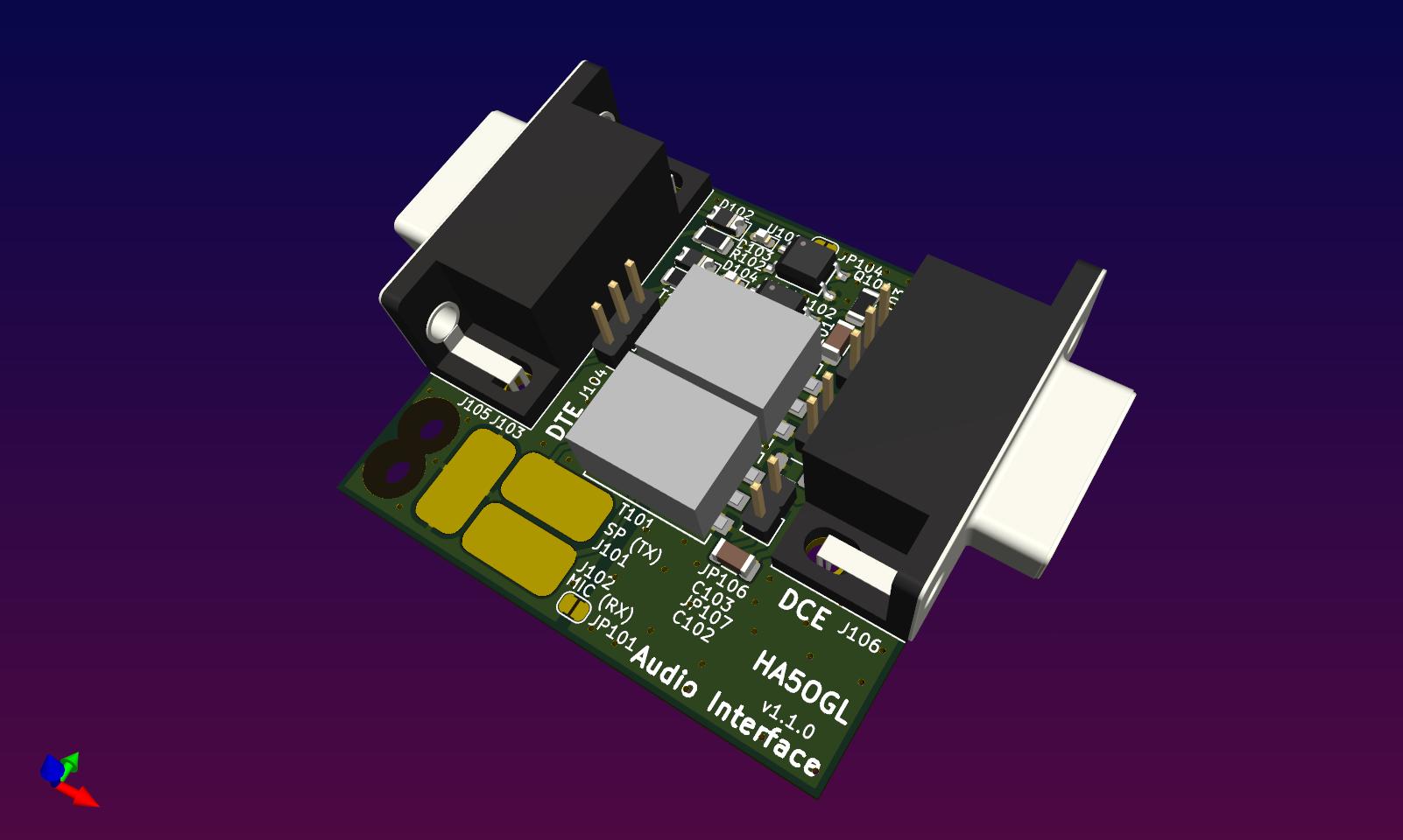
This device was designed to connect amateur radios to computers to operate digital modes.
This device works well with the following programs and user cases.
The schematic. Click on the image to download as PDF.
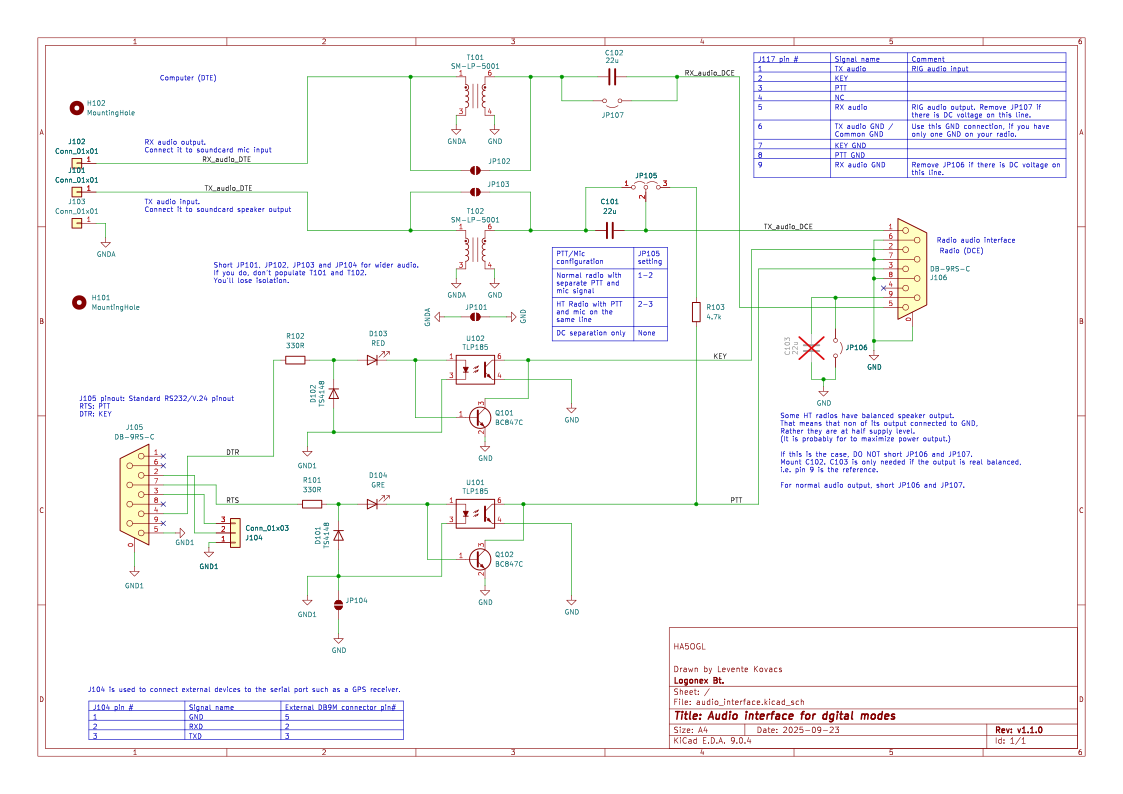
The devices is equipped with a DB-9F connector that connects to the serial port of your computer. An USB to serial converter can also be used. The DTR and RTS signals are used to key CW and PTT lines. These lines are optically isolated from the radio. There is a 3 pin header (J104) provided to connect to external serial devices such as a GPS module. LEDs are provided to monitor PTT and CW activity.
Audio signals are routed through audio transformers to provide galvanic isolation. DC blocking capacitors can be introduced to the audio paths both on the RX and TX loop at the radio (DCE) side. This is especially useful, if the device is used with HT (handheld transceiver) radio, which often uses balanced speaker output with DC offset. (Like the FT-4X.)
There are three GND connection in the board.
GNDA and GND1 can be shorted together using solderable jumpers JP101 and JP104 respectively. It is only advised to short grounds when no isolation is needed.
Soldering pads.
| Signal name | Connection | Comment |
|---|---|---|
| RX audio | J102 | To the mic input of the soundcard |
| TX audio | J101 | To the speaker output of the soundcard |
| GND | J103 | GND |
This is a standard RS232/V.24 pinout using DB9F connector.
3 pin header. This might be wired to an external DB9M connector. You obviously loose control lines, but in most cases, they are not needed anyays.
| Signal name | Pin# | Pin# of external connector DB9M | Comment |
|---|---|---|---|
| GND | 1 | 5 | |
| RXD | 2 | 2 | |
| TXD | 3 | 3 |
DB9F connector.
| Signal name | Pin# | Comment |
|---|---|---|
| TX audio | 1 | RIG audio input |
| KEY | 2 | |
| PTT | 3 | |
| NC | 4 | No connection |
| RX audio | 5 | RIG audio output. Remove JP107 if there is DC voltage on this line. |
| TX audio GND / Common GND | 6 | |
| KEY GND | 7 | KEY GND |
| PTT GND | 8 | |
| RX audio GND | 9 | Remove JP106 if there is DC voltage on this line. |
Adjust R103 if PTT is not triggered with your HT.
Measure the current through R101 and R102. (Practically, by measuring the voltage on the resistor, and applying Ohm's law.)
Adjust R101/R102 if your current is over 7mA, or under 4mA.
Set PTT output to RTS, and CW key to DTR.
| Qty | Value | Footprint | References |
|---|---|---|---|
| 4 | SolderJumper_2_Open | Jumper:SolderJumper-2_P1.3mm_Open_RoundedPad1.0x1.5mm | JP101, JP102, JP103, JP104 |
| 3 | 22u | Capacitor_SMD:C_1206_3216Metric | C101, C102, C103 |
| 3 | Conn_01x01 | Connector_Wire:SolderWirePad_1x01_SMD_5x10mm | J101, J102, J103 |
| 2 | 330R | Resistor_SMD:R_1206_3216Metric | R101, R102 |
| 2 | BC847C | Package_TO_SOT_SMD:SOT-23 | Q101, Q102 |
| 2 | DB-9RS-C | Connector_Dsub:DSUB-9_Female_Horizontal_P2.77x2.84mm_EdgePinOffset7.70mm_Housed_MountingHolesOffset9.12mm | J105, J106 |
| 2 | MountingHole | l_mounting_hole:l_MountingHole_Clear_2.75mm_M2.5 | H101, H102 |
| 2 | SM-LP-5001 | l_transformer:SM_LP_5001 | T101, T102 |
| 2 | TLP185 | l_optocoupler:11-4M1S | U101, U102 |
| 2 | TS4148 | Diode_SMD:D_1206_3216Metric | D101, D102 |
| 2 | ~ | Connector_PinHeader_2.54mm:PinHeader_1x02_P2.54mm_Vertical | JP106, JP107 |
| 1 | 4.7k | Resistor_SMD:R_1206_3216Metric | R103 |
| 1 | Conn_01x03 | Connector_PinHeader_2.54mm:PinHeader_1x03_P2.54mm_Vertical | J104 |
| 1 | GRE | LED_SMD:LED_0603_1608Metric | D104 |
| 1 | RED | LED_SMD:LED_0603_1608Metric | D103 |
| 1 | ~ | Connector_PinHeader_2.54mm:PinHeader_1x03_P2.54mm_Vertical | JP105 |
It measures 50 × 45 mm and has 2 copper layers, 1.6 mm thick.
31 parts, built around the TLP185, BC847C, SM-LP-5001 and TS4148. The full list of its parts is on this page, with links to each part's symbol and footprint where PCBKit's library has them.
From the leventelist/audio_interface repository on GitHub, at the commit this page was made from: the board is hw/audio_interface.kicad_pcb and its schematic hw/audio_interface.kicad_sch. PCBKit opens the board in the browser, with nothing to install.
Its repository states no licence, so its author keeps all rights: ask leventelist before reusing the design.

project802/ic-705_audio_interface
This project was done as a learning exercise for me, and a way to have some fun. I wanted to use my IC-705 with just an iPhone to drive digital mode communications, but limitations of both the radio and the phone meant…

brucemack/microlink
An open source EchoLink/AllStarLink implementation that runs on a simple microcontroller.

myriadrf/reference-development-kit
The Myriad-RF Reference Hardware design files and firmware

myriadrf/STREAM
FPGA development platform for high-performance RF and digital design


