2 layers105 × 135 mm
 gianlucarenzi/Vera-Module-RBL-XE
[WORK IN PROGRESS - NOT WORKING] VERA video/audio module for ATARI XL/XE (PBI / cartridge, ESP32-S3 + iCE40)
VERA MODULE RBL is an open-source printed circuit board by gianlucarenzi, from the gianlucarenzi/Vera-Module-RBL-XE repository on GitHub, published under the GPL-3.0 licence. It is a 4-layer board of 143 × 162.5 mm with 219 parts on 245 nets, routed with 2,709 tracks and 572 vias.
It is built around the ESP32-S3FN8, ICE40UP5K-SG48ITR50 and W25Q16JVSNIQ, with the WM8524CGEDT, MAX40200AUK and SN74LVC00AD among its other parts. Its parts include 77 resistors, 69 capacitors, 22 ICs, 7 connectors and 3 transistors. It belongs with the retro computing and games and audio and music boards and the ESP32 and FPGA and CPLD boards of this library.


 [blocked]


🌐 English | 🌐 Italiano
[!WARNING] WORK IN PROGRESS — NOT WORKING. This project is under development and does not work yet. The board has not been built or tested; firmware (ESP32, FPGA) and documentation have only been checked in simulation or on paper and may contain errors. Do not manufacture the PCB or rely on this design yet.
The VERA Module RBL-XE is a sophisticated FPGA-based audio and video expansion card designed specifically for ATARI XE computers. This module brings modern graphics and audio capabilities to classic ATARI systems through the PBI (Parallel Bus Interface) protocol connectors.
VERA (Video Enhanced Retro Adapter) is originally designed for the Commander X16 computer but has been adapted for ATARI systems. It provides:
| Component | Specification |
|---|---|
| FPGA | Lattice ICE40UP5K-SG48ITR |
| Microcontroller | ESP32-S3FN8 |
| Flash Memory | W25Q16JVSNIQ (16Mbit) |
| Audio Codec | WM8524CGEDT |
| USB Interface | CH340T |
| Power Regulators | AMS1117-3.3V, AMS1117-1.2V, L7805 |
| Crystal (VERA board) | 25 MHz ECS-2033-250-BN (ICE40UP5K reference clock) |
| Crystal (ESP32-S3) | 40 MHz external — required; XTAL_P (QFN56 pin 54) / XTAL_N (pin 53) |
| PCB Layers | 4-layer (Signal/Power/GND/Signal) |
| Board Size | TBD mm x TBD mm |
| Parameter | Min | Typ | Max | Unit |
|---|---|---|---|---|
| Supply Voltage | 4.5 | 5.0 | 5.5 | V |
| Current Consumption | - | 800 | 1200 | mA |
| Operating Temperature | -10 | 25 | 70 | °C |
| VGA Output Impedance | - | 75 | - | Ω |
| Audio Output Level | - | 2.0 | - | Vrms |
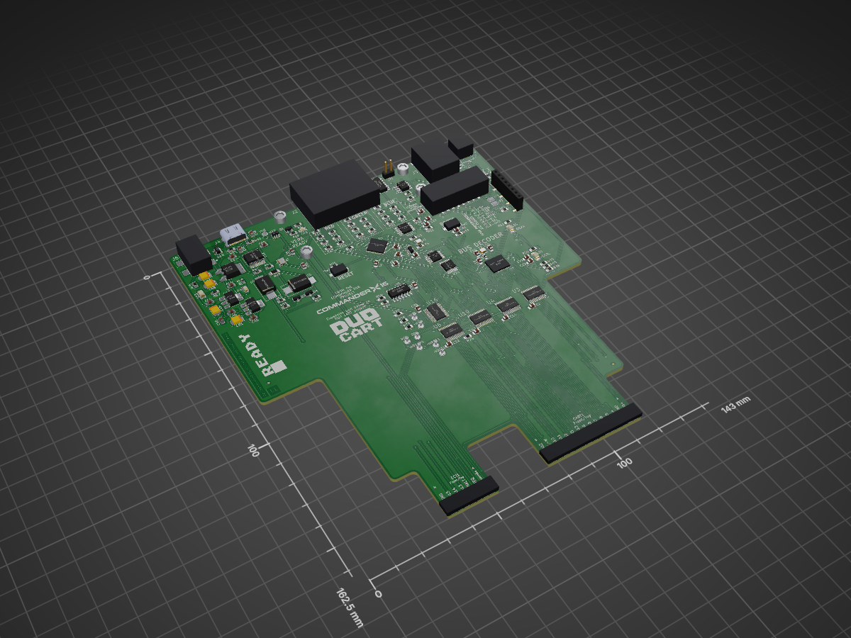
ee.get_gpio_in / ee.wr_mask_gpio_out, 1 CPU cycle) within the 279 ns PHI2-high window of the 1.79 MHz 6502 clock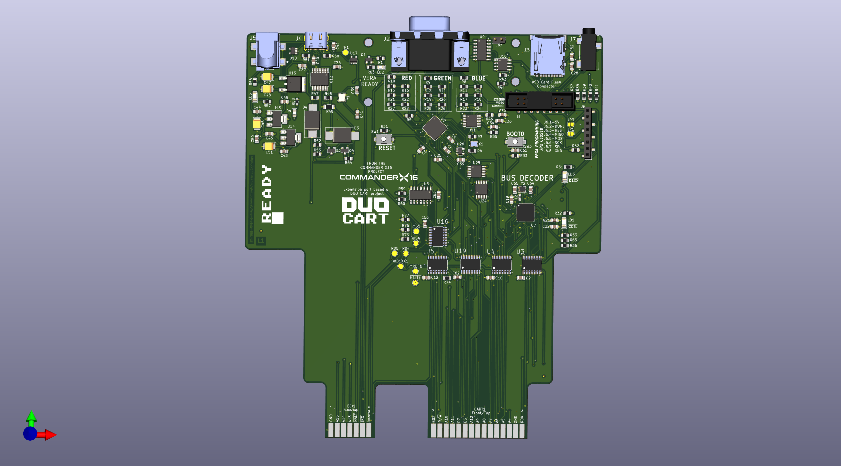 Top side showing main components and connectors
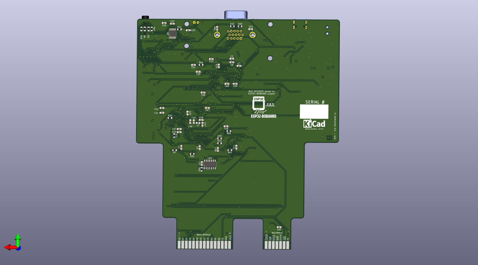 Bottom side with additional components
 Optional cartridge interface adapter
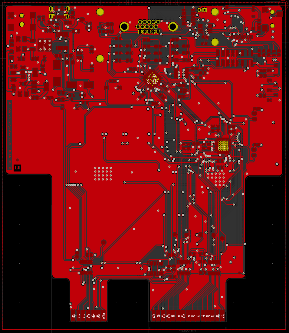 Component placement and signal routing
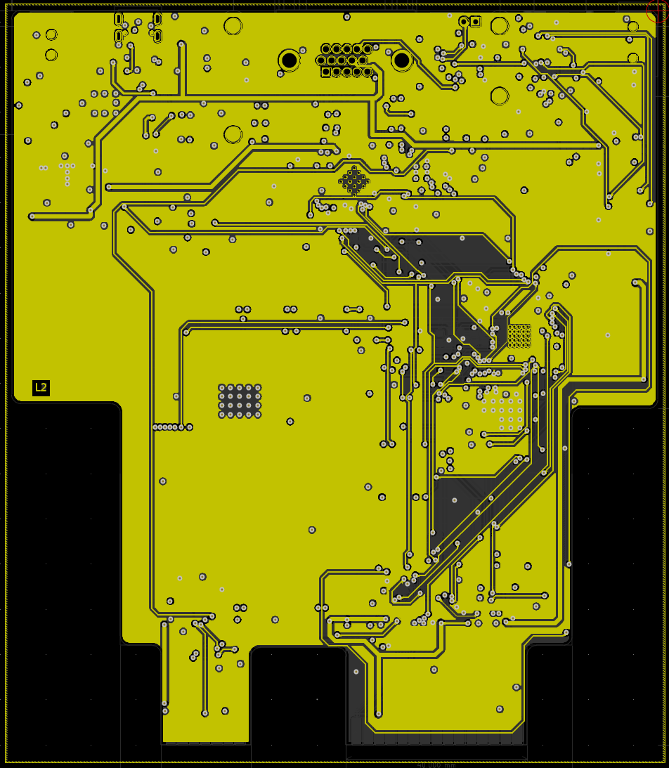 5V, 3.3V, and 1.2V power distribution
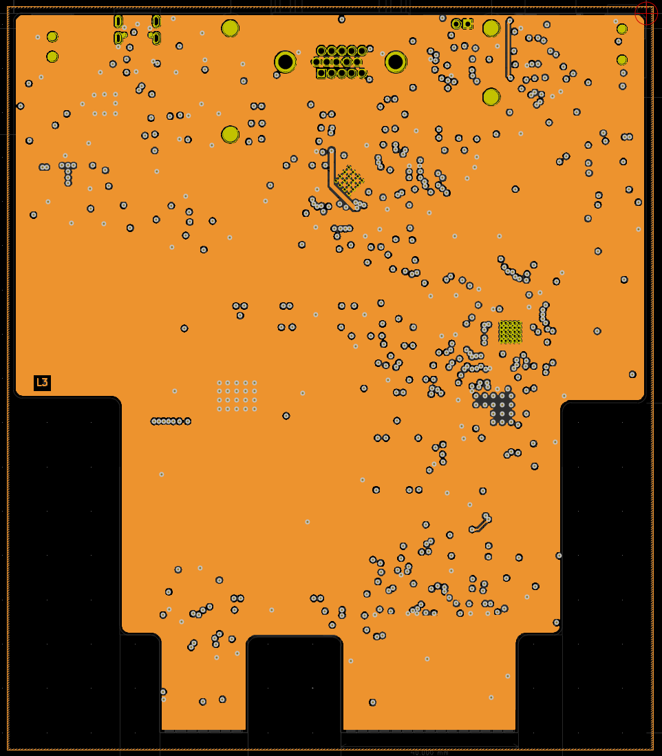 Solid ground plane for signal integrity
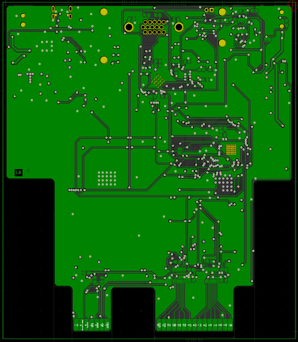 Additional signal routing and components
| Pin | Signal | Description |
|---|---|---|
| 1-3 | RGB | Red, Green, Blue analog signals |
| 13-14 | H/V Sync | Horizontal/Vertical sync |
| 6-10 | GND | Ground connections |
| 11-12 | Audio L/R | Stereo audio output |
⚠ Program the board only when it is unplugged from the Atari. The board 5 V rail is tied to the Atari +5 V (cartridge pin 13, ECI pin 7) without a diode: with the USB cable (J4) or the DC jack (J5) connected while the board is in the Atari, the board would power a switched-off Atari or run in parallel with its supply. The same applies to the serial monitor: inside the Atari use a USB adapter without VBUS. See
VERA-ATARI-HW-REQUIREMENTS.md§2.11.
| Pin | Signal | Function |
|---|---|---|
| 1 | 5V | Power supply |
| 2 | FPGA_CDONE/PULL-UP | FPGA Programmed |
| 3 | FPGA_RESET | FPGA Reset |
| 4 | MISO | SPI data in |
| 5 | MOSI | SPI data out |
| 6 | SCK | SPI clock |
| 7 | SS | SPI select |
| 8 | GND | Ground |
| Rail | Voltage | Current | Components |
|---|---|---|---|
| 5V | 5.0V ± 5% | 200mA | Input from ATARI, USB |
| 3.3V | 3.3V ± 3% | 400mA | ESP32, logic, interfaces |
| 1.2V | 1.2V ± 3% | 300mA | FPGA core voltage |
| Category | Estimated Cost | Percentage |
|---|---|---|
| FPGA | $15-20 | 35% |
| ESP32 | $8-12 | 20% |
| Connectors | $5-8 | 15% |
| Passives | $3-5 | 10% |
| PCB | $8-12 | 20% |
| Total | $39-57 | 100% |
Costs are estimates for small quantity production
# Install icestorm toolchain
sudo apt install fpga-icestorm

# Program FPGA via USB (The FPGA bitstream is not provided!)
iceprog vera_module.bin

# Verify programming
iceprog -cThe ESP32-S3FN8 (Core 0 hot loop, Core 1 serial log) handles:
setup() (before Serial.begin). MonitorTask releases CRESET, polls CDONE until the ICE40UP5K bitstream is loaded (< 100 ms typical, 5 s timeout), then releases ARESET — Atari starts with bus and FPGA already readyee.wr_mask_gpio_out, 1 CPU cycle) within the 279 ns PHI2-high windowGPIO.out for ROM ($D800–$DFFF) and RAM ($D600–$D7FF) reads; FPGA drives the bus in CCTL modeThe operating mode is selected at compile time via VERA_BOARD_IS_PBI in main.cpp:
VERA_BOARD_IS_PBI | Mode | Active ranges | Selection latch |
|---|---|---|---|
1 (default) | PBI | $D100–$D1FF, $D600–$D7FF, $D800–$DFFF | write 0x80 to $D1FF |
0 | CCTL | $D500–$D5FF | write 0x80 to $D5FF |
The RAMbo 256 KB emulator is always compiled in and enabled at runtime via GPIO 3
(PIN_RAMBO_EN, QFN56 pin 8) — no recompilation needed:
| GPIO 3 at boot | Effect |
|---|---|
| Pull-up 10 kΩ → VCC (HIGH) | RAMbo enabled — 256 KB bank-switched at $4000–$7FFF; PORTB ($D301) bit 4 selects active/inactive |
| Pull-down 10 kΩ → GND (LOW) | RAMbo disabled — $4000–$7FFF not intercepted |
Works in both PBI and CCTL mode. The hot loop snoops both PBCTL ($D303) and
PORTB ($D301): writes to $D301 update the bank-selection register only when
PBCTL bit 2 = 1 (output register selected). When bit 2 = 0, $D301 addresses the PIA
6520 DDR and the write is ignored for bank-switching purposes. PORTB initialises to
0xFF (RAME = 1, RAMbo inactive); PBCTL to 0x00 (bit 2 = 0, DDR exposed).
Passive snooping vs. active driving — no conflict with the physical 6520. The real
6520 PIA chip remains fully active on the Atari motherboard and responds to $D301/$D303
normally. The ESP32 does not replace the 6520 — it only snoops those bus cycles
(observes without driving). It only actively drives the data bus and asserts EXTSEL_N
for the $4000–$7FFF window, where the 6520 is not mapped. PBCTL tracking is necessary
precisely because the snooping is passive: from the bus, a DDR write and an Output Register
write to $D301 are indistinguishable — PBCTL state is the only way to tell them apart.
The firmware is built with PlatformIO (install via pip install platformio):
# Build firmware (edit VERA_BOARD_IS_PBI in main.cpp before building)
pio run -e esp32s3fn8

# Flash firmware — connect UART adapter to GPIO43/44
pio run -e esp32s3fn8 --target uploadNote: USB CDC is disabled because GPIO 19 (USB D−) and GPIO 20 (USB D+) are reused as address lines A7 and A8. Use an external UART adapter on GPIO 43/44.
The design workflow, from the schematic to the JLCPCB order (stock check, library update, ERC, netlist, PCB and net classes, DRC, output_job.sh, files to send), is described in WORKFLOW.md (in Italian, also as PDF).
Vera-Module-RBL-XE/
├── 📄 README.md                    # This documentation
├── 📄 WORKFLOW.md                  # Design workflow, schematic to JLCPCB order
├── 📄 PIN-MAPPING.md               # ESP32-S3 / level-shifter pin mapping
├── 📄 VERA-ATARI-HW-REQUIREMENTS.md # Hardware requirements & bring-up plan (from driver/emulator work)
├── 📄 LICENSE                      # GPL v3 license
├── ⚙️ VERA-MODULE-RBL.pro         # KiCad project file
├── 📄 VERA-MODULE-RBL.sch         # Main schematic
├── 🔧 VERA-MODULE-RBL.kicad_pcb   # PCB layout
├── 📄 VERA-MODULE-RBL.csv         # Bill of materials
├── 🐍 jlcpcb-check-bom.py        # BOM processing script
├── 📁 images/                      # Board images and renders
│   ├── 🖼️ VERA-MODULE-RBL-TOP.png
│   ├── 🖼️ VERA-MODULE-RBL-BOTTOM.png
│   ├── 🖼️ F.Cu-L1.png            # PCB layer images
│   ├── 🖼️ POWER-L2.png
│   ├── 🖼️ GND-L3.png
│   └── 🖼️ B.Cu-L4.png
├── 📁 production/                  # Manufacturing files
│   ├── 📄 *.gbl, *.gtl            # Gerber files
│   ├── 📄 *.drl                   # Drill files
│   └── 📄 *.gbrjob                # Job files
├── 📁 ibom/                       # Interactive BOM
│ └── 🌐 ibom.htmlVERA-ATARI-HW-REQUIREMENTS.md — what the VERA FPGA
requires from the bus, open points on this board (U19 output enable, WR hold time,
push-pull IRQ), the gating logic for the data-bus transceiver output enable,
reset/configuration sequence and the bring-up test plan.This project is licensed under the GNU General Public License v3.0.
For the complete license text, see the LICENSE file.
If you find this project useful, please consider:
🌟 Starring the repository
🐛 Reporting issues
🔧 Contributing improvements
📢 Sharing with the community
Made with ❤️ by RetroBit Lab
Bringing modern capabilities to classic computers
🌐 English | 🌐 Italiano
[!WARNING] LAVORO IN CORSO — NON FUNZIONANTE. Il progetto è in fase di sviluppo e non funziona ancora. La scheda non è stata realizzata né provata; firmware (ESP32, FPGA) e documentazione sono stati verificati solo in simulazione o sulla carta e possono contenere errori. Non produrre il PCB e non fare affidamento su questo progetto.
Il VERA Module RBL-XE è una sofisticata scheda di espansione audio e video basata su FPGA, progettata specificamente per i computer ATARI XE. Questo modulo porta capacità grafiche e audio moderne ai sistemi ATARI classici attraverso i connettori cartuccia ed ECI per il supporto del protocollo PBI (Parallel Bus Interface).
VERA (Video Enhanced Retro Adapter) è originariamente progettato per il computer Commander X16 ma è stato adattato per i sistemi ATARI. Fornisce:
| Componente | Specifica |
|---|---|
| FPGA | Lattice ICE40UP5K-SG48ITR |
| Microcontrollore | ESP32-S3FN8 |
| Memoria Flash | W25Q16JVSNIQ (16Mbit) |
| Codec Audio | WM8524CGEDT |
| Interfaccia USB | CH340T |
| Regolatori Alimentazione | AMS1117-3.3V, AMS1117-1.2V, L7805 |
| Cristallo (scheda VERA) | 25 MHz ECS-2033-250-BN (clock di riferimento ICE40UP5K) |
| Cristallo (ESP32-S3) | 40 MHz esterno — obbligatorio; XTAL_P (QFN56 pin 54) / XTAL_N (pin 53) |
| Layer PCB | 4 layer (Segnale/Alimentazione/GND/Segnale) |
| Dimensioni Scheda | TBD mm x TBD mm |
| Parametro | Min | Tip | Max | Unità |
|---|---|---|---|---|
| Tensione Alimentazione | 4.5 | 5.0 | 5.5 | V |
| Consumo Corrente | - | 800 | 1200 | mA |
| Temperatura Operativa | -10 | 25 | 70 | °C |
| Impedenza Uscita VGA | - | 75 | - | Ω |
| Livello Uscita Audio | - | 2.0 | - | Vrms |
Lato superiore mostrando componenti principali e connettori
Lato inferiore con componenti aggiuntivi
Adattatore interfaccia cartuccia opzionale
Posizionamento componenti e routing segnali
Distribuzione alimentazione 5V, 3.3V e 1.2V
Piano massa solido per integrità segnale
Routing segnali aggiuntivo e componenti
| Pin | Segnale | Descrizione |
|---|---|---|
| 1-3 | RGB | Segnali analogici Rosso, Verde, Blu |
| 13-14 | H/V Sync | Sync orizzontale/verticale |
| 6-10 | GND | Connessioni massa |
| 11-12 | Audio L/R | Uscita audio stereo |
| Pin | Segnale | Funzione |
|---|---|---|
| 1 | 5V | Alimentazione |
| 2 | FPGA_CDONE/PULL-UP | FPGA Programmata |
| 3 | FPGA_RESET | FPGA Reset |
| 4 | MISO | Dati SPI in ingresso |
| 5 | MOSI | Dati SPI in uscita |
| 6 | SCK | Clock SPI |
| 7 | SS | Selezione SPI |
| 8 | GND | Ground |
| Rail | Tensione | Corrente | Componenti |
|---|---|---|---|
| 5V | 5.0V ± 5% | 200mA | Ingresso da ATARI, USB |
| 3.3V | 3.3V ± 3% | 400mA | ESP32, logica, interfacce |
| 1.2V | 1.2V ± 3% | 300mA | Tensione core FPGA |
| Categoria | Costo Stimato | Percentuale |
|---|---|---|
| FPGA | $15-20 | 35% |
| ESP32 | $8-12 | 20% |
| Connettori | $5-8 | 15% |
| Passivi | $3-5 | 10% |
| PCB | $8-12 | 20% |
| Totale | $39-57 | 100% |
I costi sono stime per produzione piccole quantità
# Installare toolchain icestorm
sudo apt install fpga-icestorm

# Programmare FPGA via USB (Il bitstream FPGA non e' fornito!)
iceprog vera_module.bin

# Verificare programmazione
iceprog -cL'ESP32-S3FN8 (hot loop sul Core 0, log seriale sul Core 1) gestisce:
setup() (prima di Serial.begin). MonitorTask rilascia CRESET, attende CDONE = HIGH (bitstream ICE40UP5K caricato, tipicamente < 100 ms, timeout 5 s), poi rilascia ARESET — l'Atari parte con bus e FPGA già operativiee.wr_mask_gpio_out, 1 ciclo CPU) nella finestra PHI2-high di 279 nsGPIO.out per letture ROM ($D800–$DFFF) e RAM ($D600–$D7FF); in modalità CCTL è la FPGA a guidare il busLa modalità operativa è scelta a tempo di compilazione tramite VERA_BOARD_IS_PBI in main.cpp:
VERA_BOARD_IS_PBI | Modalità | Range attivi | Latch selezione |
|---|---|---|---|
1 (default) | PBI | $D100–$D1FF, $D600–$D7FF, $D800–$DFFF | write 0x80 su $D1FF |
0 | CCTL | $D500–$D5FF | write 0x80 su $D5FF |
L'emulatore RAMbo 256 KB è sempre compilato nel firmware e abilitato a runtime tramite
GPIO 3 (PIN_RAMBO_EN, QFN56 pin 8) — nessuna ricompilazione necessaria:
| GPIO 3 al boot | Effetto |
|---|---|
| Pull-up 10 kΩ → VCC (HIGH) | RAMbo abilitato — 256 KB bank-switched a $4000–$7FFF; bit 4 di PORTB ($D301) seleziona attivo/inattivo |
| Pull-down 10 kΩ → GND (LOW) | RAMbo disabilitato — $4000–$7FFF non intercettato |
Funziona in entrambe le modalità PBI e CCTL. Il hot loop snoopa sia PBCTL ($D303)
sia PORTB ($D301): le write a $D301 aggiornano il registro di selezione banco
solo se PBCTL bit 2 = 1 (Output Register selezionato). Quando bit 2 = 0, $D301
indirizza il DDR della PIA 6520 e la write viene ignorata. PORTB si inizializza a
0xFF (RAME = 1, RAMbo inattivo); PBCTL a 0x00 (bit 2 = 0, DDR esposto).
Snooping passivo vs. pilotaggio attivo — nessun conflitto col 6520 fisico. Il chip
6520 PIA rimane pienamente attivo sulla scheda madre dell'Atari e risponde a $D301/$D303
normalmente. L'ESP32 non sostituisce il 6520: osserva passivamente quei cicli bus senza
mai pilotare il bus dati per quegli indirizzi. Pilota attivamente D0–D7 e asserisce
EXTSEL_N solo per la finestra $4000–$7FFF, dove il 6520 non è mappato. Il tracciamento
di PBCTL è necessario proprio perché lo snooping è passivo: dal bus, una write al DDR e una
write all'Output Register su $D301 sono indistinguibili — lo stato di PBCTL è l'unico
modo per differenziarle.
Il firmware viene compilato con PlatformIO (installare con pip install platformio):
# Compila firmware (modificare VERA_BOARD_IS_PBI in main.cpp prima di compilare)
pio run -e esp32s3fn8

# Carica firmware — adattatore UART su GPIO43/44
pio run -e esp32s3fn8 --target uploadNota: USB CDC è disabilitato perché GPIO 19 (USB D−) e GPIO 20 (USB D+) sono riutilizzati come linee indirizzo A7 e A8. Usare un adattatore UART esterno su GPIO 43/44.
Il workflow di progetto, dallo schematico all'ordine JLCPCB (disponibilità dei componenti, aggiornamento della libreria, ERC, netlist, PCB e netclass, DRC, output_job.sh, file da consegnare), è descritto in WORKFLOW.md (anche in PDF).
Vera-Module-RBL-XE/
├── 📄 README.md                    # Questa documentazione
├── 📄 WORKFLOW.md                  # Workflow di progetto, dallo schema all'ordine JLCPCB
├── 📄 LICENSE                      # Licenza GPL v3
├── ⚙️ VERA-MODULE-RBL.pro         # File progetto KiCad
├── 📄 VERA-MODULE-RBL.sch         # Schema principale
├── 🔧 VERA-MODULE-RBL.kicad_pcb   # Layout PCB
├── 📄 VERA-MODULE-RBL.csv         # Distinta materiali
├── 🐍 jlcpcb-check-bom.py        # Script elaborazione BOM
├── 📁 images/                      # Immagini scheda e render
│   ├── 🖼️ VERA-MODULE-RBL-TOP.png
│   ├── 🖼️ VERA-MODULE-RBL-BOTTOM.png
│   ├── 🖼️ F.Cu-L1.png            # Immagini layer PCB
│   ├── 🖼️ POWER-L2.png
│   ├── 🖼️ GND-L3.png
│   └── 🖼️ B.Cu-L4.png
├── 📁 production/                  # File produzione
│   ├── 📄 *.gbl, *.gtl            # File Gerber
│   ├── 📄 *.drl                   # File drill
│   └── 📄 *.gbrjob                # File job
├── 📁 ibom/                       # BOM interattiva
│   └── 🌐 ibom.html
└── 📁 schematics/                 # Schemi individuali
├── 📄 vera-fpga.sch # Modulo FPGAQuesto progetto è licenziato sotto la GNU General Public License v3.0.
Per il testo completo della licenza, vedere il file LICENSE.
Se trovi utile questo progetto, considera di:
🌟 Mettere una stella al repository
🐛 Segnalare problemi
🔧 Contribuire miglioramenti
📢 Condividere con la community
Realizzato con ❤️ da RetroBit Lab
Portando capacità moderne ai computer classici
| Qty | Value | Footprint | References |
|---|---|---|---|
| 35 | 100nF | Capacitor_SMD:C_0805_2012Metric_Pad1.18x1.45mm_HandSolder | C1, C2, C10, C11, C12, C14, C16, C18, C20, C22, C23, C27, C28, C29, C38, C40 +19 |
| 15 | 1uF | Capacitor_SMD:C_0805_2012Metric_Pad1.18x1.45mm_HandSolder | C3, C4, C5, C6, C7, C8, C25, C30, C31, C32, C33, C43, C59, C60, C66 |
| 13 | 10K | Resistor_SMD:R_0805_2012Metric_Pad1.20x1.40mm_HandSolder | R5, R7, R34, R36, R47, R48, R53, R62, R63, R65, R69, R70, R71 |
| 10 | CREZ08051% | Resistor_SMD:R_0805_2012Metric_Pad1.20x1.40mm_HandSolder | R35, R56, R64, R66, R72, R73, R74, R75, R76, R77 |
| 8 | 47K | Resistor_SMD:R_0805_2012Metric_Pad1.20x1.40mm_HandSolder | R37, R38, R39, R40, R41, R42, R43, R44 |
| 7 | TestPoint | TestPoint:TestPoint_Pad_D2.0mm | ~HALT1, ~mREF1, ~mS4, ~mS5, mD1XX1, RD4, RD5 |
| 6 | 10uF | Capacitor_SMD:C_0805_2012Metric_Pad1.18x1.45mm_HandSolder | C13, C15, C17, C19, C21, C24 |
| 5 | 74LVC4245APW_118 | RetroBitLab:IC_74LVC4245_SOP65P640X110-24N | U3, U4, U6, U16, U19 |
| 4 | 4K7 | Resistor_SMD:R_0805_2012Metric_Pad1.20x1.40mm_HandSolder | R31, R33, R59, R60 |
| 4 | 510R | Resistor_SMD:R_0805_2012Metric_Pad1.20x1.40mm_HandSolder | R23, R25, R27, R57 |
| 4 | 560R | Resistor_SMD:R_0805_2012Metric_Pad1.20x1.40mm_HandSolder | R45, R46, R67, R68 |
| 4 | Fiducial | Fiducial:Fiducial_0.5mm_Mask1mm | FID1, FID2, FID3, FID4 |
| 4 | MountingHole | MountingHole:MountingHole_3.2mm_M3 | H1, H2, H3, H4 |
| 3 | 10uF-20V | Capacitor_Tantalum_SMD:CP_EIA-3528-12_Kemet-T_Pad1.50x2.35mm_HandSolder | C45, C48, C51 |
| 3 | 150R | Resistor_SMD:R_0805_2012Metric_Pad1.20x1.40mm_HandSolder | R12, R14, R16 |
| 3 | 160R | Resistor_SMD:R_0805_2012Metric_Pad1.20x1.40mm_HandSolder | R18, R20, R22 |
| 3 | 27R | Resistor_SMD:R_0805_2012Metric_Pad1.20x1.40mm_HandSolder | R24, R26, R28 |
| 3 | 2K | Resistor_SMD:R_0805_2012Metric_Pad1.20x1.40mm_HandSolder | R11, R13, R15 |
| 3 | 4.7uF | Capacitor_SMD:C_0805_2012Metric_Pad1.18x1.45mm_HandSolder | C26, C34, C35 |
| 3 | 4K3 | Resistor_SMD:R_0805_2012Metric_Pad1.20x1.40mm_HandSolder | R8, R9, R10 |
| 3 | 910R | Resistor_SMD:R_0805_2012Metric_Pad1.20x1.40mm_HandSolder | R17, R19, R21 |
| 3 | RED | LED_SMD:LED_1206_3216Metric_Pad1.42x1.75mm_HandSolder | LD1, LD3, LD5 |
| 2 | 1K | Resistor_SMD:R_0805_2012Metric_Pad1.20x1.40mm_HandSolder | R2, R6 |
| 2 | 20pF | Capacitor_SMD:C_0805_2012Metric_Pad1.18x1.45mm_HandSolder | C39, C41 |
| 2 | 27pF | Capacitor_SMD:C_0805_2012Metric_Pad1.18x1.45mm_HandSolder | C64, C65 |
| 2 | 2K2 | Resistor_SMD:R_0805_2012Metric_Pad1.20x1.40mm_HandSolder | R52, R55 |
| 2 | 330R | Resistor_SMD:R_0805_2012Metric_Pad1.20x1.40mm_HandSolder | R32, R61 |
| 2 | 50R | Resistor_SMD:R_0805_2012Metric_Pad1.20x1.40mm_HandSolder | R3, R4 |
| 2 | 5K1 | Resistor_SMD:R_0805_2012Metric_Pad1.20x1.40mm_HandSolder | R50, R51 |
| 2 | 820R | Resistor_SMD:R_0805_2012Metric_Pad1.20x1.40mm_HandSolder | R29, R30 |
| 2 | BC817,SOT-23 | Package_TO_SOT_SMD:SOT-23 | Q3, Q4 |
| 2 | DIOSCH20V | Diode_SMD:D_SMC_Handsoldering | D3, D4 |
| 2 | GREEN | LED_SMD:LED_0805_2012Metric_Pad1.15x1.40mm_HandSolder | LD2, LD4 |
| 2 | MAX40200AUK | Package_TO_SOT_SMD:SOT-23-5 | U17, U18 |
| 2 | SN74LVC00 | Package_SO:TSSOP-14_4.4x5mm_P0.65mm | U24, U25 |
| 2 | SPST2P | RetroBitLab:SPST-7.3x3.9x2.5-WUERTH-434121025816 | SW1, SW3 |
| 2 | SolderJumper_2_Open | Jumper:SolderJumper-2_P1.3mm_Open_RoundedPad1.0x1.5mm | JP1, JP3 |
| 1 | 10uF-35V | Capacitor_Tantalum_SMD:CP_EIA-3528-12_Kemet-T_Pad1.50x2.35mm_HandSolder | C47 |
| 1 | 12MHzC | Crystal:Crystal_SMD_EuroQuartz_MT-4Pin_3.2x2.5mm | Y1 |
| 1 | 2.2uF | Capacitor_SMD:C_0805_2012Metric_Pad1.18x1.45mm_HandSolder | C36 |
| 1 | 220R | Resistor_SMD:R_0805_2012Metric_Pad1.20x1.40mm_HandSolder | R54 |
| 1 | 22uF | Capacitor_SMD:C_0805_2012Metric_Pad1.18x1.45mm_HandSolder | C37 |
| 1 | 2K7 | Resistor_SMD:R_0805_2012Metric_Pad1.20x1.40mm_HandSolder | R1 |
| 1 | 330R | Resistor_SMD:R_0603_1608Metric_Pad0.98x0.95mm_HandSolder | R58 |
| 1 | 40.000Mhz | Crystal:Crystal_SMD_2520-4Pin_2.5x2.0mm | Y2 |
| 1 | 74CBTLV3126PW,118 | Package_SO:TSSOP-14_4.4x5mm_P0.65mm | U8 |
| 1 | AMS1117-1.2 | Package_TO_SOT_SMD:SOT-223-3_TabPin2 | U14 |
| 1 | AMS1117-3.3 | Package_TO_SOT_SMD:SOT-223-3_TabPin2 | U13 |
| 1 | ATARI DUO BUS | RetroBitLab:DUOCart_20x11_Rev | LOGO4 |
| 1 | ATARI READY | RetroBitLab:atari_ready_8mm_rev | LOGO2 |
| 1 | ATARI-CARTRIDGE | RetroBitLab:ATARI-LEFT-CARTRIDGE | CART1 |
| 1 | CD4011B | Package_SO:SOIC-14_3.9x8.7mm_P1.27mm | U9 |
| 1 | CONN_DM3AT-SF-PEJM5 | RetroBitLab:HRS_DM3AT-SF-PEJM5 | J3 |
| 1 | CONN_SMD_01x08_Staggered_2.54mm | Connector_PinSocket_2.54mm:PinSocket_1x08_P2.54mm_Vertical_SMD_Pin1Right | J6 |
| 1 | CONN_SMD_HEADER_BOX_02x08_HX-JN2.54 | RetroBitLab:IDC-Header_2x08_P2.54mm_Vertical_SMD | J1 |
| 1 | DNP | Resistor_SMD:R_1206_3216Metric_Pad1.30x1.75mm_HandSolder | R49 |
| 1 | DS1038-15FBNSiA74-0CC | RetroBitLab:CONNFLY_DS1038-15FBNSIA74-0CC | J2 |
| 1 | DX07S016JA1R1500 | RetroBitLab:JAE_DX07S016JA1R1500 | J4 |
| 1 | ECIBUS | RetroBitLab:ATARI-XE-ECI-SLOT | ECI1 |
| 1 | ESP32-S3FN8 | RetroBitLab:IC_ESP32-S3FN8-QFN40P700X700X90-57N | U7 |
| 1 | ESP32_BOBOARD | RetroBitLab:ESP32_BOBOARD_5V_21.7mmx21.7mm | LOGO5 |
| 1 | FB0805100R100MHZ4A | Inductor_SMD:L_0805_2012Metric_Pad1.15x1.40mm_HandSolder | L1 |
| 1 | IC74HC00 | Package_SO:SOIC-14_3.9x8.7mm_P1.27mm | U5 |
| 1 | ICE40UP5K-SG48ITR | RetroBitLab:QFN-48-1EP_7x7mm_P0.5mm_EP5.6x5.6mm | U2 |
| 1 | IND0603600R100MHZ300mA | Inductor_SMD:L_0603_1608Metric_Pad1.05x0.95mm_HandSolder | L2 |
| 1 | Jumper_2_Open | Connector_PinHeader_2.54mm:PinHeader_1x02_P2.54mm_Vertical | JP2 |
| 1 | KiCAD DESIGN | Symbol:KiCad-Logo2_6mm_SilkScreen | LOGO3 |
| 1 | L7805 | Package_TO_SOT_SMD:TO-252-2 | U15 |
| 1 | Label-20mmx10mm | RetroBitLab:Label-20mmx10mm-Silkscreen | LBL1 |
| 1 | MOSFET-BSS138-SOT-23 | Package_TO_SOT_SMD:SOT-23 | Q1 |
| 1 | OT3EL89CJI-111YLC-25M | RetroBitLab:OSC_ECS-2033-250-BN | X1 |
| 1 | PJ-002AH-SMT-TR | RetroBitLab:CUI_PJ-002AH-SMT-TR | J5 |
| 1 | PJ-313D | RetroBitLab:jack_3.5_pj313d-smt | J7 |
| 1 | SN74HCT04DR | Package_SO:SOIC-14_3.9x8.7mm_P1.27mm | U23 |
| 1 | SN74LVC1G07DBVR | Package_TO_SOT_SMD:SOT-23-5 | U26 |
| 1 | TP5V | TestPoint:TestPoint_Pad_D2.0mm | TP1 |
| 1 | USBCH340T | RetroBitLab:SSOP-20_5.3x7.2mm_P0.65mm_Pad0.45 | U12 |
| 1 | VERA X16 LOGO | RetroBitLab:x16logo | LOGO1 |
| 1 | W25Q16JVSNIQ | Package_SO:SOIC-8_3.9x4.9mm_P1.27mm | U10 |
| 1 | WM8524CGEDT | Package_SO:TSSOP-16_4.4x5mm_P0.65mm | U11 |


ifilot/open-vera-module
VERA (Versatile Embedded Retro Adapter) is a self-contained FPGA video and audio module for retro-computing projects.

Maverick-Shark/X65_BigMiST
The X65 is an ultimate computer for everyone interested in the venerable 65-series of 8-bit and 16-bit CPUs, i.e. the 6502 and 65816.


trope-oshw/anthracite
MIDI-controllable fuzz pedal: open hardware (CERN-OHL-S-2.0), firmware (GPL-3.0-or-later)


It measures 143 × 162.5 mm and has 4 copper layers, 1.6 mm thick.
219 parts, built around the ESP32-S3FN8, ICE40UP5K-SG48ITR50, W25Q16JVSNIQ and WM8524CGEDT. The full list of its parts is on this page, with links to each part's symbol and footprint where PCBKit's library has them.
From the gianlucarenzi/Vera-Module-RBL-XE repository on GitHub, at the commit this page was made from: the board is VERA-MODULE-RBL.kicad_pcb. PCBKit opens the board in the browser, with nothing to install.
Its repository publishes it under the GPL-3.0 licence: you may reuse it on that licence's terms (keep the author's notice, and for a copyleft licence share your changes alike).