2 layers
Z parts
fl4p/Fugu2
Links: git | kicanvas | cadlab | docs | pdf schematics | IBOM (TODO) | firmware | additional docs & resources
14 parts24

 fl4p/Fugu224
Links: git | kicanvas | cadlab | docs | pdf schematics | IBOM (TODO) | firmware | additional docs & resources
Fugu2 is an open-source printed circuit board by fl4p, from the fl4p/Fugu2 repository on GitHub. It is a 2-layer board of 58.5 × 88 mm with 147 parts on 80 nets, routed with 988 tracks and 172 vias.
It is built around the ESP32-S3-WROOM-1-N4, SN74LVC1G125DBVR-TP and AP3012KTR-G1, with the UCC21330BQDRQ1, SN74LVC1G17DBVR and LESD5D5.0CT1G among its other parts. Its parts include 44 resistors, 35 capacitors, 16 diodes, 9 transistors and 7 connectors. It belongs with the ESP32 boards of this library.


Links: git | kicanvas | cadlab | docs | pdf schematics | IBOM (TODO) | firmware | additional docs & resources
TODO 3d web rendering
gate drv considerations:
- separate gate discharge diode?
- eval gate drv voltage?
- pull down for each fet? 10k pull down?
usb-c: select 12V instead of 5V


final points:
- what about the LS diodes? SMD and TO220, do power measurements.
    - ST15100S and ...
    - 2nd LS switch parallel ?
- sw push footprint
- test without TVS diodes at solar voltage divider. when does the mcu die?
- tune dead-time


bom opts:
- Cin: C11, C22 replace with MSASH32MSB5475MPCA01 / HMK325BJ475MM-PE ?
cheaper and specifically for SMPS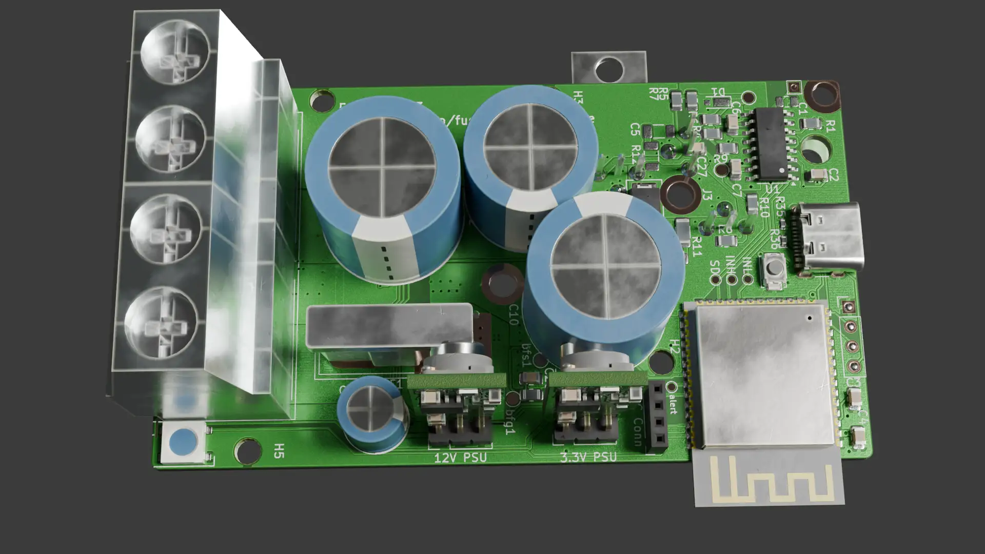 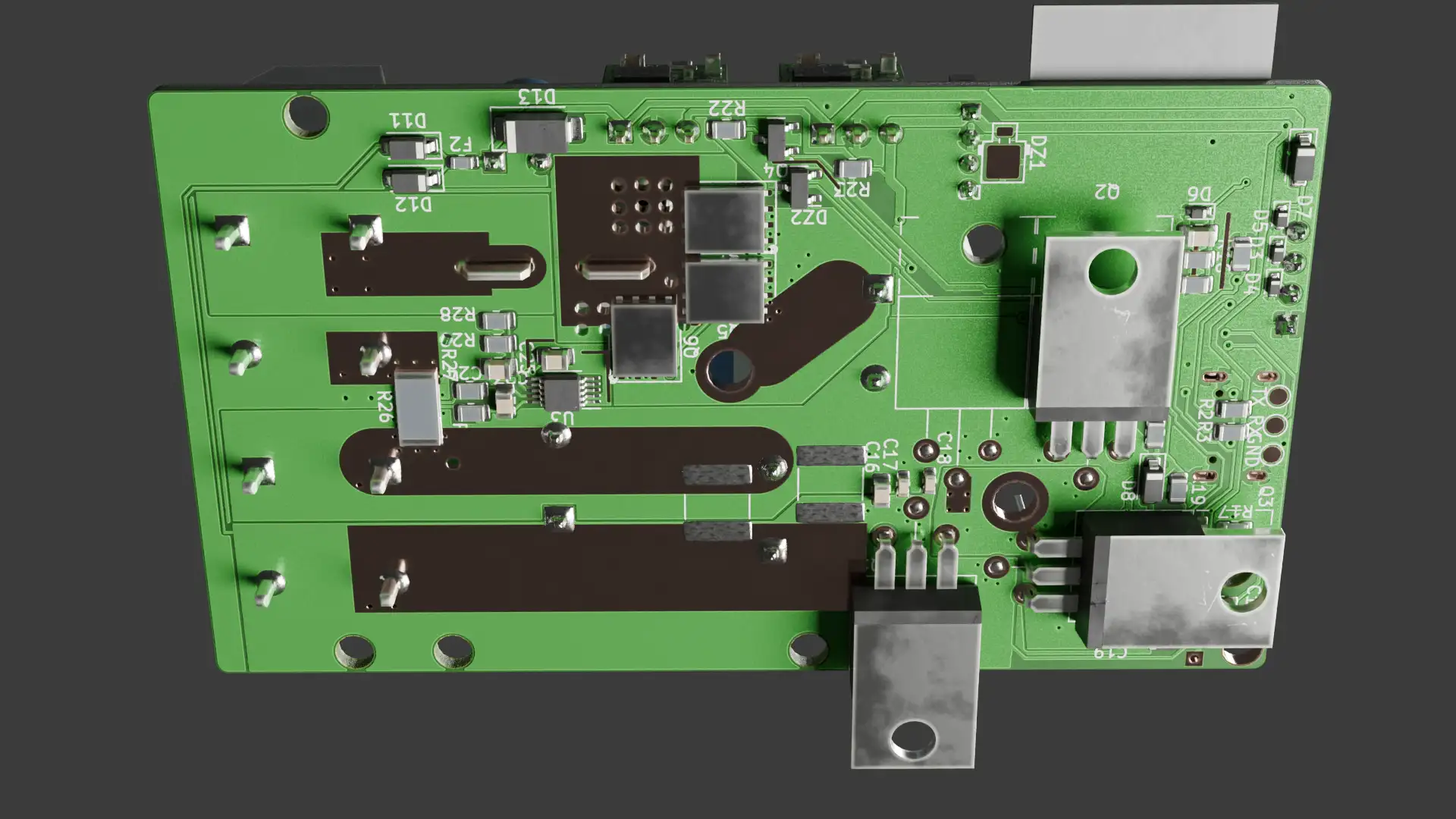 |
|---|
| Current Hardware v2.3 rendering with USB type-C port and large terminal blocks (top & bottom) |
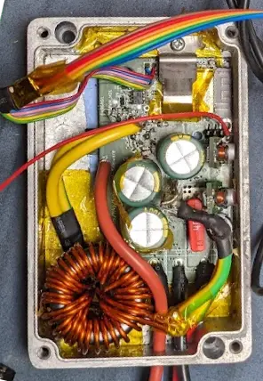 | 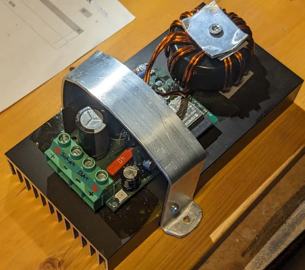 |
|---|---|
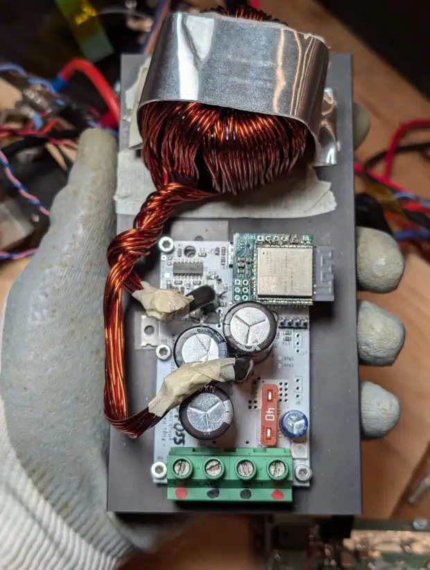
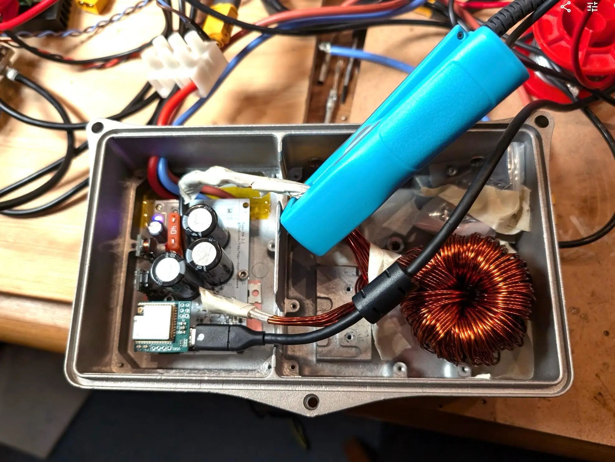
| Small aluminium enclosure with two T130 sendust coil cores fmetal | mounted on heatsink, T184 sendust core fheat |
This is inspired by Fugu MPPT. The design has been optimized with real life experience, considering signal noise and EMI issues, replaced hall sensor with shunt resistor and faster switching. See the list below for more changes.
You can place the ESP32-S3 directly on the board and use the USB pin header or the ESP-PROG header for flashing. Alternatively, you can place SMD pin headers where the ESP32-S3 footprint is and use the MCU header board. This makes it easier to replace the MCU in case it breaks. You can of course create your own header board using another MCU series such as the STM32.
Fugu2.kicad_pcbpsu/buck100.kicad_pcb (for 3.3V supply)mcu-head/Fugu2-esp32s3-wroom-head.kicad_pcb (optional. this allows easy replacement of the ESP32S3 during
development. alternatively place the ESP32(-S3) directly on the Fugu2 board)Fugu2/
and kikit-packer/ in the same directory. then run panelize.sh (linux, mac) or panelize.bat (windows). It
will generate combined.kicad_pcb which you can send to your PCB manufacturer.The inductor should have an inductivity value that is high enough to keep the ripple current in range, a common design rule is that ripple is in the range of 0.3 ~ 0.5 of the dc current. Notice that inductivity decreases with dc bias current. The dc bias current is the average current through the coil. This means that the higher the output current of the converter, the lower the inductivity. This causes the AC indcutor ripple current to rise faster than linear with higher currents. High ripple currents cause more loss in the inductor core (hysteresis loss) and capacitors (parasitic ESR). Going beyond the safe limits can cause extremely high peak currents leading to destruction of the FETs.
The micrometals design tool is a good starting point to find suitable inductor designs with mostly toroid cores. It gives the user recommendations on core shape, core material and wire (diameter and strands).
Off-the-shelf inductors exists, however they are usually expensive (>$20), such as the CODACA CPEX4141L-500MC (optimized for dc bias / saturation current) and CPEA4141L-500MC (optimized for low loss). On LCSC you'll find Ruishen RSEQ32-470M, RSEQ3635-460M and RSEQ3635-700M. I have only tested toe CODACA cores and no experience with the LCSC parts.
Diving into inductor design can be overwhelming at first. In practice there is no perfect inductor for a specific application. Given current, voltage and temperature contraints, the designer usually optimizes for one or more goals, which always comes with trade-offs. In short:
Winding an inductor is nothing to worry about and is actually fun. Below you'll find two design proposals, one for 12 and 24V, upto 40A and the other for 48V batteries. Before, let's have a short intro to better understand the design decisions.
A well designed inductor has a core/copper loss ratio between 50/50 and 20/80 (micrometals). Copper is easier to cool than the core. With higher DC output current the core material magnetization increases and inductivity value drops. A good design has a maximum drop of ~50% of its initial inductivity. Lower inductivity will cause higher ripple current, which will cause more loss in the core and capacitors (increased AC amplitude of magnetic field and current).
For higher DC currents chose a larger core (or materials optimized for DC saturation, which can have low availability and a higher price tag). For higher output voltage chose a higher inductivity value.
Sendust (KoolMµ) is a magnetic core material commonly used for power applications. It is affordable with high availability, has good saturation characteristics and low loss. Manufacturers offer optimized materials, tuning for price, dc bias and/or core loss. (KDM: KPH, KAM, KAH, KH)
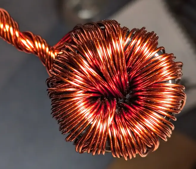
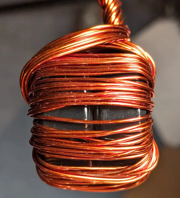
For the coil winding choose isolated Copper wire made for electrical applictions commonly referred as W210 with typical conductivity of 58.5 MS/m. Choose diameter and number of strands so that inner diameter of the toroid core has a good usage. Prefer multiple strands for easier winding (>2mm diameter becomes unhandy to wind) and reduced ac loss (skin & proximity effects). Many strands (>10) increase complexity of winding. A diameter between 1 and 2mm appears to be good choice. More copper reduces dc resistance and leakage fringing (TODO ref). Evenly wind the wire on the core to reduce leakage fringing.
In a nutshell, the LS switch should have low Rds_on, low Qrr, low Qgd (low self turn-on). The HS switch should have low Qsw. See Toshibas Product Guide on pg. 16.
Use fetlib for an extensive parametric search and ranking by power loss estimation.
Current through the LS Switch always flows from source to drain (4th quadrant of V-I plane), which makes the gate drive signal rather irrelevant. It is much easier to switch than the HS, ringing is generally not an issue. TI Gate Drive Fudamentals Switching happens near zero voltage, as the body diode is usually already/still conducting when switching on/off.
Choose a MOSFET that is designed for synchronous rectification. Consider switch node ringing and choose a higher voltage fet to avoid channel break-down if needed.
Schematics.pdf is regenerated on commit whenever a .kicad_sch file is staged, via
a tracked git hook in .githooks/. The refreshed PDF is left unstaged — stage and
commit it yourself (git add Schematics.pdf) when you want it in history. After a fresh
clone, activate the hook once:
git config core.hooksPath .githooksThe hook needs kicad-cli on the PATH (or the default macOS KiCad app bundle). If
kicad-cli is unavailable it is skipped and the commit proceeds unchanged.
| Qty | Value | Footprint | References |
|---|---|---|---|
| 11 | 10k | Resistor_SMD:R_0805_2012Metric | R2, R3, R8, R9, R13, R14, R15, R16, R23, R45, R46 |
| 5 | 100nF, X7R, 25V | Capacitor_SMD:C_0805_2012Metric | C2, C4, C6, C7, C35 |
| 5 | 200k | Resistor_SMD:R_0805_2012Metric | R17, R18, R21, R43, R44 |
| 5 | LESD5D5.0CT1G | Diode_SMD:D_SOD-523 | D3, D4, D6, D20, D21 |
| 5 | SS310 | Diode_SMD:D_SOD-123 | D7, D8, D10, D11, D12 |
| 4 | 1000uF, 100V | Capacitor_THT:CP_Radial_D18.0mm_P7.50mm | C10, C11, C12, C34 |
| 4 | 100nF, 25V | Capacitor_SMD:C_0805_2012Metric | C1, C29, C36, C37 |
| 4 | 1uF, 100V, X7S | Capacitor_SMD:C_0805_2012Metric | C9, C14, C16, C27 |
| 4 | MountingHole | MountingHole:MountingHole_3.2mm_M3_DIN965 | H2, H3, H4, H5 |
| 3 | 10nF, 100V | Capacitor_SMD:C_0805_2012Metric | C15, C20, C31 |
| 3 | 1k | Resistor_SMD:R_0805_2012Metric | R39, R40, R51 |
| 3 | 4.7, 1% | Resistor_SMD:R_0805_2012Metric | R4, R6, R10 |
| 3 | 5.1k 1% | Resistor_SMD:R_0402_1005Metric | R35, R36, R38 |
| 3 | TPH1R306PL,L1Q or NTMFS5C612NLT1G | open-pe:Infineon_PG-TDSON-8_FL | Q5, Q6, Q7 |
| 3 | ~ | TestPoint:TestPoint_Pad_D1.5mm | bfg1, bfs1, TPHO1 |
| 2 | 10uF, 100V, X7S | Capacitor_SMD:C_1210_3225Metric_Pad1.33x2.70mm_HandSolder | C21, C22 |
| 2 | 10uF, 16V | Capacitor_SMD:C_0805_2012Metric | C19, C28 |
| 2 | 1uF, 10V, X7S | Capacitor_SMD:C_0805_2012Metric | C3, C30 |
| 2 | 2.2, 1% | Resistor_SMD:R_0805_2012Metric | R5, R7 |
| 2 | 220 | Resistor_SMD:R_0805_2012Metric | R48, R49 |
| 2 | 220nF, 100V, X7S | Capacitor_SMD:C_0603_1608Metric | C17, C18 |
| 2 | 691256610002 | open-pe:TerminalBlock_WR-TBL_2566_1x02_P10.16mm | J9, J10 |
| 2 | 7.5 | Resistor_SMD:R_1206_3216Metric | R11, R12 |
| 2 | BSS123 | Package_TO_SOT_SMD:SOT-23 | Q4, Q9 |
| 2 | GND | TestPoint:TestPoint_Pad_D1.5mm | TP3, TP3 |
| 2 | IPA050N10NM5S | open-pe:TO-220-3_Horizontal_BottomHeatsink_SmallHole | Q1, Q3 |
| 2 | RX | TestPoint:TestPoint_Pad_D1.5mm | TP1, TP1 |
| 2 | TX | TestPoint:TestPoint_Pad_D1.5mm | TP2, TP2 |
| 1 | 0.0005 | open-pe:R_2512_6332Metric_Pad2.72x3.40mm_HandSolder | R26 |
| 1 | 100k | Resistor_SMD:R_0805_2012Metric | R47 |
| 1 | 100nF | Capacitor_SMD:C_0805_2012Metric | C26 |
| 1 | 100pF | Capacitor_SMD:C_0805_2012Metric | C32 |
| 1 | 10uH | Inductor_SMD:L_0805_2012Metric_Pad1.15x1.40mm_HandSolder | L2 |
| 1 | 11k, 1% | Resistor_SMD:R_0805_2012Metric | R53 |
| 1 | 1M | Resistor_SMD:R_0805_2012Metric | R24 |
| 1 | 1uF, X7R, 25V | Capacitor_SMD:C_0805_2012Metric | C33 |
| 1 | 2.2nF, 200V, X7S | Capacitor_SMD:C_1206_3216Metric | C5 |
| 1 | 2.2nF, 200V, X7S | Capacitor_SMD:C_0805_2012Metric_Pad1.18x1.45mm_HandSolder | C8 |
| 1 | 20k | Resistor_SMD:R_0805_2012Metric | R1 |
| 1 | 22 | Resistor_SMD:R_0805_2012Metric | R19 |
| 1 | 226k, 1% | Resistor_SMD:R_0805_2012Metric | R42 |
| 1 | 25A 58V | open-pe:Fuse_Blade_Mini_directSolderThin | F3 |
| 1 | 3.3V PSU | Connector_PinHeader_2.54mm:PinHeader_1x03_P2.54mm_Vertical | J7 |
| 1 | 33k | Resistor_SMD:R_0805_2012Metric | R37 |
| 1 | 4.7uF, 100V | Capacitor_SMD:C_1210_3225Metric_Pad1.33x2.70mm_HandSolder | C13 |
| 1 | 40A | open-pe:Fuse_Blade_ATO_directSolderThin | F1 |
| 1 | 43k, 1% | Resistor_SMD:R_0805_2012Metric | R41 |
| 1 | 470k, 1% | Resistor_SMD:R_0805_2012Metric | R52 |
| 1 | 470uF | Capacitor_THT:CP_Radial_D18.0mm_P7.50mm | C12 |
| 1 | 47k | Resistor_SMD:R_0805_2012Metric | R50 |
| 1 | 47k, 1% | Resistor_SMD:R_0805_2012Metric | R22 |
| 1 | 62V | Package_TO_SOT_SMD:SOT-23-3 | D18 |
| 1 | 7.5k | Resistor_SMD:R_0805_2012Metric | R20 |
| 1 | AP3012 | Package_TO_SOT_SMD:SOT-23-5 | U5 |
| 1 | AS333 | Package_TO_SOT_SMD:SOT-353_SC-70-5 | U6 |
| 1 | BZT52C13-TP | Diode_SMD:D_SOD-123 | DZ2 |
| 1 | Conn_L_SW | open-pe:SolderWire-1x01_D3.5mm | J3 |
| 1 | Conn_L_out | open-pe:SolderWire-1x01_D3.5mm | J6 |
| 1 | ESP32-S3-WROOM-1-N4 | open-pe:ESP32-S3-WROOM-1-noPIN15 | U2 |
| 1 | GT800N10D3 | open-pe:VSON-8_3.3x3.3mm_P0.65mm_NexFET | Q8 |
| 1 | INH | TestPoint:TestPoint_Pad_D1.0mm | TPINH1 |
| 1 | INL | TestPoint:TestPoint_Pad_D1.0mm | TPINL1 |
| 1 | IPP022N12NM6 | open-pe:TO-220-3_Horizontal_BottomHeatsink_NoHole | Q2 |
| 1 | MCU head | open-pe:PinHeader_2x07_P2.54mm_Vertical_SMD_Pin1Left | J4 |
| 1 | MSS1P4-M3/89A | Diode_SMD:D_SOD-323 | D17 |
| 1 | MSS1P4-M3/89A | Diode_SMD:D_MicroSMP_AK | D1 |
| 1 | MountingHole | MountingHole:MountingHole_3.2mm_M3_DIN965_Pad_TopOnly | H1 |
| 1 | NCP18XH103F03RB | Resistor_SMD:R_0603_1608Metric_Pad0.98x0.95mm_HandSolder | TH1 |
| 1 | QTGM027 | open-pe:USB_C_Receptacle_GCT_USB4105-xx-A_16P_TopMnt_Horizontal | P2 |
| 1 | SD | TestPoint:TestPoint_Pad_D1.0mm | TPSD1 |
| 1 | SM2T3V3A | PCM_Diode_SMD_AKL:D_Powermite_KA | DZ1 |
| 1 | SMAJ85A | Diode_SMD:D_SMA | D13 |
| 1 | SMD1206B010TF/60 or 500mA fast, 50A | Fuse:Fuse_1206_3216Metric_Pad1.42x1.75mm_HandSolder | F2 |
| 1 | SN74LVC1G125DBVR | Package_TO_SOT_SMD:SOT-23-5 | U7 |
| 1 | SN74LVC1G17DBVR | Package_TO_SOT_SMD:SOT-23-5 | U8 |
| 1 | ST15100S | open-pe:TO-277B_ThermalVias | D16 |
| 1 | ST40100C | open-pe:TO-220-3_Horizontal_BottomHeatsink_NoHole | D9 |
| 1 | SW_Push | Button_Switch_SMD:SW_Push_SPST_NO_Alps_SKRK | SW1 |
| 1 | TP_PWM_LO | TestPoint:TestPoint_Pad_D1.5mm | TPLO1 |
| 1 | UCC21330BQDRQ1 | Package_SO:SOIC-16_3.9x9.9mm_P1.27mm | U1 |
The 143 most common of 147 parts.
fl4p/Fugu2
Links: git | kicanvas | cadlab | docs | pdf schematics | IBOM (TODO) | firmware | additional docs & resources


SK-Electronics-Consulting/electronics-widgets
Small, Custom Tools for Electronics

EPFLXplore/XRE_LeggedRobot_HW
PCB designs for Xplore Research's robot dog project

dognotdog/smol_servo
circuitry and software for controlling NEMA17 size brushless motors and stepper motors as servos.
It measures 58.5 × 88 mm and has 2 copper layers, 1.6 mm thick.
147 parts, built around the ESP32-S3-WROOM-1-N4, SN74LVC1G125DBVR-TP, AP3012KTR-G1 and UCC21330BQDRQ1. The full list of its parts is on this page, with links to each part's symbol and footprint where PCBKit's library has them.
From the fl4p/Fugu2 repository on GitHub, at the commit this page was made from: the board is Fugu2.kicad_pcb and its schematic ExtPort.kicad_sch. PCBKit opens the board in the browser, with nothing to install.
Its repository states no licence, so its author keeps all rights: ask fl4p before reusing the design.