2 layers59.4 × 35.8 mm

 fjalvingh/km11
PDP-11 KM11 maintenance module, using an LCD screen
Km1105 is an open-source printed circuit board by fjalvingh, from the fjalvingh/km11 repository on GitHub. It is a 2-layer board of 131.7 × 80 mm with 46 parts on 114 nets, routed with 2,135 tracks and 215 vias.
It is built around the ATTINY1616-SN, SN74LVC245APW and PCF8574T, with the 74ACT00SC and BC547 among its other parts. Its parts include 12 capacitors, 10 resistors, 10 ICs, 5 connectors and 2 diodes. It belongs with the lEDs and displays boards and the AVR (ATmega, ATtiny) boards of this library.


This is supposed to become a KM11 maintenance module. It is a 2 slot card which should be placed in both KM11 slots of a PDP 11/05 or 11/10. It uses an ATTINY1616 (or 3216 if I cannot make the code fit) and a set of i2c I/O adapters (PCF8574T) to read the data from both slots for the KM11, and writes those to an LCD screen, offset on a cable.
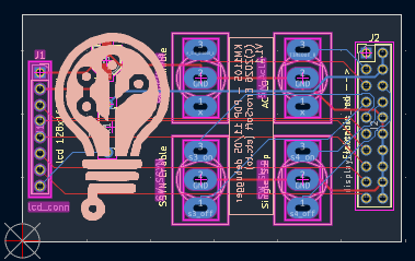
The main PCB must be placed in the PDP 11/05. The LCD display and the switches sit on
a second, small PCB (kicad/kmdisp) at the end of a 20-way ribbon cable, so they can be
outside the pdp/11 in the 3D-printed console from 3d/.
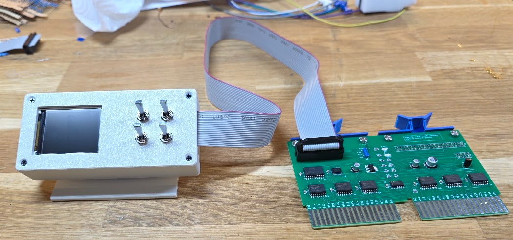
The board uses:
The first version had some small issues which were repaired in this version.
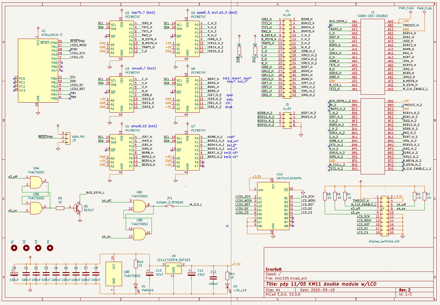
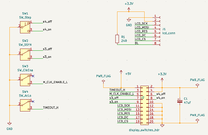
The code was partially created by Claude, and does not use the usual libraries to save space in the Flash memory of the ATTINY1616 as it only has 16K. The code directly accesses registers to control both the ST7735 LCD controller and the I2C extenders, and contains three fonts (5x7, 8x14 and 8x16).
At the time of writing the code takes about 9.3KB of the 16KB Flash available.
The code is a loop that reads all six extenders about ten times a second and repaints only what changed. The screen looks as follows:
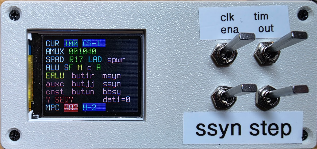
CUR 301 H-1
AMUX 000000
SPAD R7  PC  spwr
ALU SF M c A
EALU butir msyn
auxc butjj ssyn
cnst butun bbsy
E OK        dati=0
MPC 302 H-2-- until it has seen one, and again while
the clock runs.A+B+1). The function is grey when EALU is off, because then the ALU result does not reach the AMUX.I2C: followed by U numbers replaces it when an extender does not answer; the
values that extender supplies are then not real.Signals that are active low on the backplane (and shown dim on the original KM11, like the MPC and ALU S) are inverted first, so everything on the screen is the logical value. Single signals are yellow and upper case when asserted, red and lower case when negated.
Colours that mark a value:
While the processor is single stepped (M CLK ENABLE on, M CLK PULSE to step), the firmware compares the lamps with DEC's microcode listing for the microword that just executed. It checks ALU S/M/C, the scratchpad address, the four BUT lamps and AUXC. The status shows:
| Status | Meaning |
|---|---|
E OK / F OK | the lamps match the listing |
E BAD | some lamps do not match; they are drawn white on red |
SEQ? | the MPC moved to an address the previous microword cannot branch to; the MPC turns red |
-- | nothing to check: no step seen yet, or the clock is running |
The first letter is the microcode revision of the M7261: E (1973) or F (1976), or ? until
it is known. The card finds out by itself. The two revisions differ only in 14 microwords, and
the first time a step passes one of them, the AUXC lamp shows which revision is installed. Unary
instructions (CLR, INC, COM…) pass them. The revision is kept in the ATtiny's EEPROM.
make REV=E eeprom, make REV=F eeprom or make REV=AUTO eeprom sets or forgets it. Uploading
new firmware erases it, and it is learnt again.
The four switches are BUS SSYN, AC LO, M CLK PULSE (STEP) and M CLK ENABLE. The AC LO one sits
on the KM11 pin the 11/20 used for NO TIMEOUT, and the net is still called TIMEOUT_H for that
reason; on the 11/05 throwing it asserts BUS AC LO and starts the power-fail sequence.
review.md records the September 2026 check of the design and firmware against DEC's own
documentation, with the sources.
The PDP 11/05 microcode for Rev.E and Rev.F can be browsed easily using the microcode browser for the PDP 11/05.
To program the ATTINY1616 please follow the setup and instructions from my 8bit bus display tool. The source code is under src/. Two steps to do for a build:
make to build the code, thenmake upload to upload the code to the board (with the programmer connected, obviously).I made a small test setup to test driving the display:
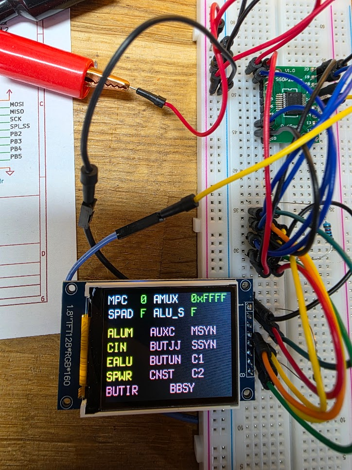
The initial idea was to use a fancy 2.25 landscape mode LCD to show the info, but after almost 4 hours of testing and messing around with the code I gave up, I assume the display I got was defective. I was not helped by the fact that the second display tested, now the 1.8" display, was ALSO found to be defective, wasting another few hours. In the end I proved that of the 5 1.8" displays I have 1 was defective, and I had to pick that one for the test, obviously. Murphy in full working order.
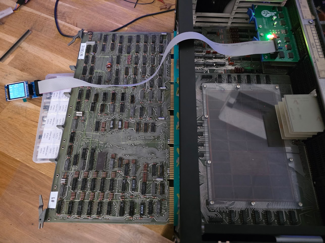
More closeup:
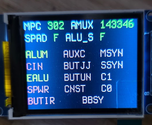 The microcode PC is at 302
oct, which is H-2, part of the HALT instruction.
The KM11 schematic in the 1973 manual shows V1 for M CLK L, the single step clock pulse. But this should be U1. The reproduction by Tony Duell properly names U1 in the ascii art schematic for S4, but misnames it as J1 in the text.
In addition the S4 remark in the same thing seems to be wrong: the clock switch should be connected the other way around (i.e. latched upward in that schematic).
| Qty | Value | Footprint | References |
|---|---|---|---|
| 9 | 100nF | Capacitor_SMD:C_0805_2012Metric | C1, C2, C3, C4, C5, C6, C7, C9, C12 |
| 8 | 1K | Resistor_SMD:R_0805_2012Metric | R4, R5, R6, R7, R8, R9, R10, R11 |
| 6 | PCF8574T | Package_SO:SOIC-16W_7.5x10.3mm_P1.27mm | U2, U3, U4, U5, U6, U7 |
| 4 | ~ | MountingHole:MountingHole_3.2mm_M3 | H1, H2, H3, H4 |
| 2 | 10uF | Capacitor_SMD:CP_Elec_4x4.5 | C10, C11 |
| 2 | 4.7k | Resistor_SMD:R_0805_2012Metric | R1, R2 |
| 1 | +3V_LED | LED_SMD:LED_1206_3216Metric_Pad1.42x1.75mm_HandSolder | D2 |
| 1 | 100uF | Capacitor_SMD:CP_Elec_6.3x7.7 | C8 |
| 1 | 74ACT00SC | Package_SO:SO-14_3.9x8.65mm_P1.27mm | U8 |
| 1 | ATtiny1616-S | Package_SO:SOIC-20W_7.5x12.8mm_P1.27mm | U1 |
| 1 | BC547 | Package_TO_SOT_THT:TO-92_Inline | Q1 |
| 1 | CONN-DEC-DOUBLE | DEC-FLIP-CHIP:CONN-DEC-DOUBLE | J1 |
| 1 | Jumper_2_Bridged | Jumper:SolderJumper-2_P1.3mm_Bridged_RoundedPad1.0x1.5mm | JP1 |
| 1 | LD1117S33TR_SOT223 | Package_TO_SOT_SMD:SOT-223-3_TabPin2 | U9 |
| 1 | LOGO | LOGO | G*** |
| 1 | PWRLED | LED_SMD:LED_1206_3216Metric_Pad1.42x1.75mm_HandSolder | D1 |
| 1 | SN74LVC245APW | Package_SO:TSSOP-20_4.4x6.5mm_P0.65mm | U10 |
| 1 | display_switches_hdr | Connector_PinHeader_2.54mm:PinHeader_2x10_P2.54mm_Vertical | J2 |
| 1 | la_01 | Connector_PinHeader_2.54mm:PinHeader_2x20_P2.54mm_Vertical | J4 |
| 1 | la_02 | Connector_PinHeader_2.54mm:PinHeader_2x04_P2.54mm_Vertical | J5 |
| 1 | pgm_hdr | Connector_PinHeader_2.54mm:PinHeader_1x03_P2.54mm_Vertical | J3 |

alan05code/Distributore
Distributore Smart | Progetto Scolastico 2023/2024 | Client (PCB) + Server(RaspBerry) + SitoWeb(HTML/CSS/JavaScript) + Simulazione(Python)


CmdrZin/chips_avr_examples
AVR assembly and C code for robotics and other projects.


fjalvingh/8bit-busdisplay
PCB for showing an 8 bit hex number from a 5V bus on a 7-segment display using an ATTINY1616

Bumb1eris/PCB_Business_Card
A coin cell powered PCB business card that can play snake

It measures 131.7 × 80 mm and has 2 copper layers, 1.6 mm thick.
46 parts, built around the ATTINY1616-SN, SN74LVC245APW, PCF8574T and 74ACT00SC. The full list of its parts is on this page, with links to each part's symbol and footprint where PCBKit's library has them.
From the fjalvingh/km11 repository on GitHub, at the commit this page was made from: the board is kicad/km1105/km1105.kicad_pcb and its schematic kicad/km1105/km1105.kicad_sch. PCBKit opens the board in the browser, with nothing to install.
Its repository states no licence, so its author keeps all rights: ask fjalvingh before reusing the design.