4 layers81.7 × 100.6 mm
Final Project PCB
ndesserich/ECE-36200-Final-Project-PCB
A PCB that integrates an RP2350 and various peripherals to play games.
80 parts1

 EvilOtter222/pcb-project
Insert later
Pcb project is an open-source printed circuit board by EvilOtter222, from the EvilOtter222/pcb-project repository on GitHub. It is a 2-layer board of 110 × 60 mm with 62 parts on 72 nets, routed with 1,027 tracks and 131 vias.
It is built around the RP2040, PAM8302AADCR and W25Q128JVSIQ, with the AP2112K-3.3 and MMBT2222A among its other parts. Its parts include 23 capacitors, 17 resistors, 10 switches, 6 connectors and 4 ICs. It belongs with the RP2040 boards of this library.


A nintendo switch inspired handheld game console I designed in KiCad, built around a bare RP2040 chip.
Hi, I'm Kai (or @relufied), a 9th grader from New Jersey passionate about all things electronics and machine learning!
This is my first PCB ever. I've done a lot of embedded stuff before (Arduino, Picos, ESP chips) and I built an 8-bit breadboard computer, but everything I've made was on breadboards and protoboards. I had never opened PCB software before this.
The idea came from a handheld I made with an ESP32 and a capacitive touch TFT (my reddit post a year ago: https://www.reddit.com/r/arduino/comments/1r4qdw3/breakout_game_with_tft_and_arduino/). I wanted to build something like that again, but with everything on one board, so the RP2040 goes straight on the PCB. I picked the RP2040 because it's cheap, it's fast-ish, and I've used it a bunch.
Made for Hack Club Half Life (week 1).
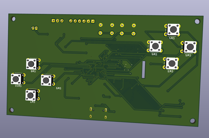
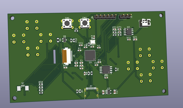
| Front | Back |
|---|---|
 |  |
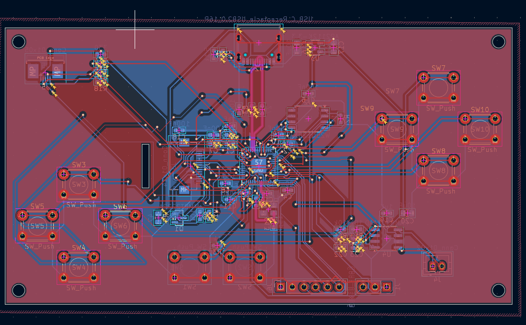
PCB:
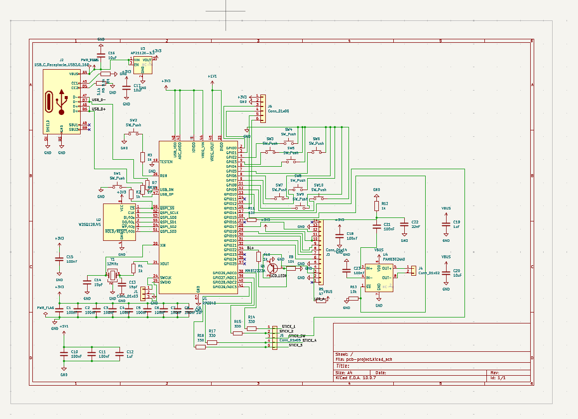
Schematic:
All the SMD parts are on the back and the front only has the buttons. There's a slot cut in the board so the display ribbon can go through to its connector on the back.
Power: USB-C gives 5V and an AP2112K regulator turns it into 3.3V for the chip, flash and display. The 5.1k resistors on the CC pins make chargers see the board as a device.
Display: SPI on GPIO17 to GPIO21. The backlight runs off 5V through a 47 ohm resistor and an NPN transistor, switched by GPIO22.
Buttons: Each one connects its pin to ground, and the firmware uses the RP2040's internal pull-ups.
Thumbstick: The stick has no datasheet, so all 4 outer ribbon pins go to GPIO26 to GPIO29 (the ADC pins) through 330 ohm resistors. The code picks which ones are power, ground, X and Y. The click goes to GPIO10. The code I gave you might not work the first time, so try swapping the order of the pins.
Sound: GPIO15 makes a PWM signal, a 10k/1k divider shrinks it, and a 22nF cap filters it before it goes into the PAM8302A. GPIO14 turns the amp on.
The test code is in firmware/firmware.ino. It's Arduino code using the Earle Philhower RP2040 core and the Adafruit ST7789 library.
It's a short and simple sanity test tests. it turns on the screen and backlight, shows which buttons are pressed, shows the thumbstick X and Y values, beeps the speaker at startup and when the stick is clicked, and sends a message out to the expansion header.
The board isn't built yet, so the code hasn't been tested. The comments will explain how to use and implement the code for each of these features.
| Pin | What it does |
|---|---|
| GPIO0, GPIO1 | Expansion header (serial) |
| GPIO2 to GPIO9 | The 8 buttons |
| GPIO10 | Thumbstick click |
| GPIO12, GPIO13 | Expansion I2C |
| GPIO14 | Amp on/off |
| GPIO15 | Audio (PWM) |
| GPIO17 to GPIO21 | Display (SPI) |
| GPIO22 | Backlight |
| GPIO26 to GPIO29 | Thumbstick |
| SWCLK, SWDIO | Debug header |
pcb-project.kicad_sch: schematicpcb-project.kicad_pcb: PCBgerbers/ and gerbers.zip: files to send to JLCPCBfirmware/: codebom.csv and BOM.md: parts listJOURNAL.md: my journal (synced from Half Life)The full list is in BOM.md and bom.csv. Parts are about $29, and about $64 with tax and shipping (estimated). The board is from JLCPCB and the parts are from LCSC, Mouser and BuyDisplay. I already had the thumbstick and speaker.
gerbers.zip (default settings, 2 layers, tented vias)The design is done. DRC shows 0 unconnected items, and 2 cosmetic errors. I did this last minute but if I had more time I would use a 40 pin tft instead of a 14 pin one.
@Shadow in even though it's normally not allowed in the Half Life huddle), but it left 27 connections it couldn't do and a mess of vias and pins that were surround by layers and layers of wires :( . I routed all 27 connections of those by hand, and next time I'm routing everything by hand.| Qty | Value | Footprint | References |
|---|---|---|---|
| 14 | 100nF | Capacitor_SMD:C_0603_1608Metric | C1, C2, C3, C4, C5, C6, C7, C8, C10, C11, C15, C18, C21, C23 |
| 10 | SW_Push | Button_Switch_THT:SW_PUSH_6mm | SW1, SW2, SW3, SW4, SW5, SW6, SW7, SW8, SW9, SW10 |
| 5 | 1k | Resistor_SMD:R_0603_1608Metric | R1, R2, R3, R10, R12 |
| 4 | 330 | Resistor_SMD:R_0603_1608Metric | R14, R15, R17, R18 |
| 3 | 10k | Resistor_SMD:R_0603_1608Metric | R8, R11, R13 |
| 3 | 10uF | Capacitor_SMD:C_0805_2012Metric | C16, C17, C20 |
| 3 | 1uF | Capacitor_SMD:C_0603_1608Metric | C9, C12, C19 |
| 2 | 15pF | Capacitor_SMD:C_0603_1608Metric | C13, C14 |
| 2 | 27 | Resistor_SMD:R_0603_1608Metric | R6, R7 |
| 2 | 5.1k | Resistor_SMD:R_0603_1608Metric | R4, R5 |
| 1 | 12MHz | Crystal:Crystal_SMD_Abracon_ABM8G-4Pin_3.2x2.5mm | Y1 |
| 1 | 22nF | Capacitor_SMD:C_0603_1608Metric | C22 |
| 1 | 47 | Resistor_SMD:R_0805_2012Metric | R9 |
| 1 | AP2112K-3.3 | Package_TO_SOT_SMD:SOT-23-5 | U3 |
| 1 | Conn_01x02 | Connector_JST:JST_PH_B2B-PH-K_1x02_P2.00mm_Vertical | J4 |
| 1 | Conn_01x03 | Connector_PinHeader_2.54mm:PinHeader_1x03_P2.54mm_Vertical | J1 |
| 1 | Conn_01x05 | Connector_FFC-FPC:TE_0-1734839-5_1x05-1MP_P0.5mm_Horizontal | J5 |
| 1 | Conn_01x06 | Connector_PinHeader_2.54mm:PinHeader_1x06_P2.54mm_Vertical | J6 |
| 1 | Conn_01x14 | Connector_FFC-FPC:Hirose_FH12-14S-0.5SH_1x14-1MP_P0.50mm_Horizontal | J3 |
| 1 | MMBT2222A | Package_TO_SOT_SMD:SOT-23 | Q1 |
| 1 | PAM8302AAD | Package_SO:SOIC-8_3.9x4.9mm_P1.27mm | U4 |
| 1 | RP2040 | Package_DFN_QFN:QFN-56-1EP_7x7mm_P0.4mm_EP3.2x3.2mm | U1 |
| 1 | USB_C_Receptacle_USB2.0_16P | Connector_USB:USB_C_Receptacle_HRO_TYPE-C-31-M-12 | J2 |
| 1 | W25Q128JVS | Package_SO:SOIC-8_5.3x5.3mm_P1.27mm | U2 |
It measures 110 × 60 mm and has 2 copper layers, 1.6 mm thick.
62 parts, built around the RP2040, PAM8302AADCR, W25Q128JVSIQ and AP2112K-3.3. The full list of its parts is on this page, with links to each part's symbol and footprint where PCBKit's library has them.
From the EvilOtter222/pcb-project repository on GitHub, at the commit this page was made from: the board is pcb-project.kicad_pcb and its schematic pcb-project.kicad_sch. PCBKit opens the board in the browser, with nothing to install.
Its repository states no licence, so its author keeps all rights: ask EvilOtter222 before reusing the design.
ndesserich/ECE-36200-Final-Project-PCB
A PCB that integrates an RP2350 and various peripherals to play games.


g210101021/OpenStylophone-RP2040
Overview • Technical Summary • Architecture • Hardware Audit & Remediation • Schematic Subsystems • PCB Layout • Firmware Roadmap • Bill of Materials • Author

fkontiebo/flight-controller
Contrôleur de vol 4 layers basé sur STM32F405RGT6, conçu comme plateforme de navigation autonome avec bus CAN.


ianklug/grooveboard
A four-key mechanical keyboard for rhythm games.