Skip to the content
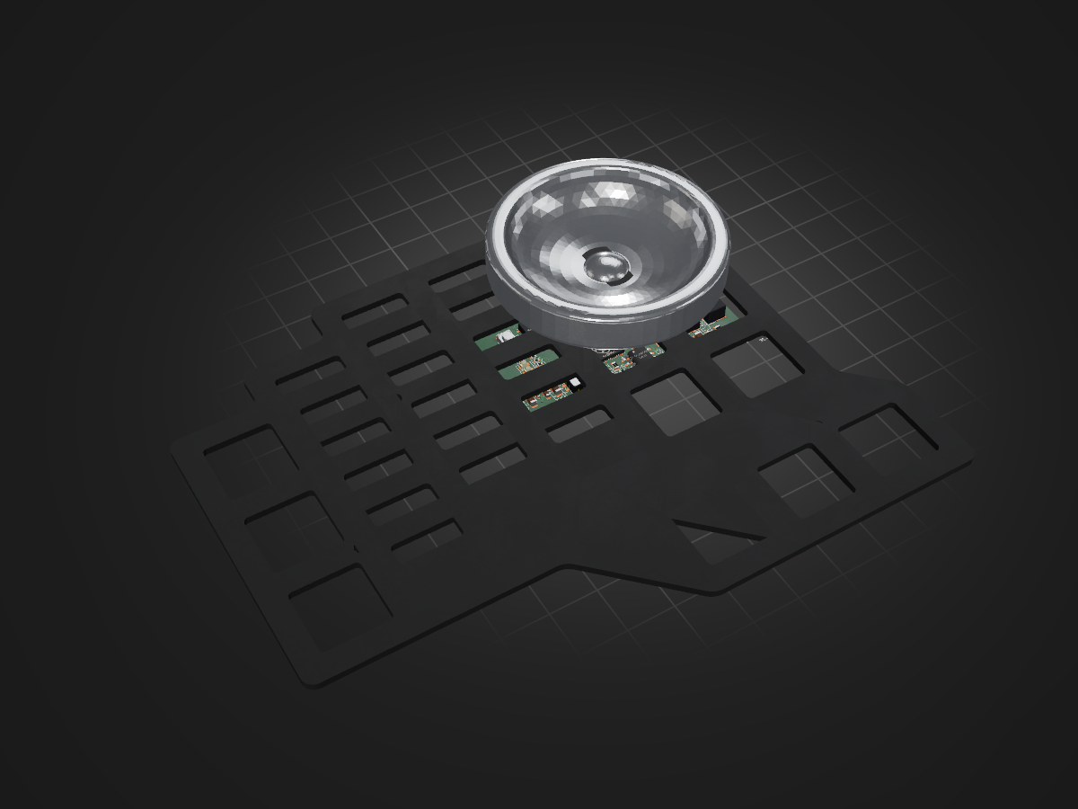
4 layers51.4 × 31.4 mmRP2350, the printed circuit board in 3D

Working notes for the first custom RP2350A board with ADXL355, USB-C development power/data, 12 V field input, RS485, and a power architecture biased toward a clean accelerometer supply.

Size
51.4 × 31.4 mm
Copper layers
4
Thickness
1.6 mm
Parts
87
Nets
89
Pads
325
Tracks, vias
661, 54
Pours
2
Routed
Yes
KiCad
KiCad 10.0 (file 20260206)
Created
21 May 2026
Updated
28 Oct 2026

Overview

RP2350 is an open-source printed circuit board by engelberd, from the engelberd/sensor-system repository on GitHub. It is a 4-layer board of 51.4 × 31.4 mm with 87 parts on 89 nets, routed with 661 tracks and 54 vias.

It is built around the RP2350A, THVD1450DRBR and W25Q128JVSIQ, with the TPS62175DQCR, ADXL355BEZ-RL7 and TLV75733PDBVR-MS among its other parts. Its parts include 17 capacitors, 14 resistors, 8 ICs, 7 diodes and 2 inductors. It belongs with the RP2350 boards of this library.

Main components

11

README

hardware/Node rev.3.5/README.md

RP2350 ADXL355 node hardware notes

Working notes for the first custom RP2350A board with ADXL355, USB-C development power/data, 12 V field input, RS485, and a power architecture biased toward a clean accelerometer supply.

Design goals

  • Keep firmware changes small by staying close to Raspberry Pi Pico 2/RP2350A.
  • Give ADXL355 the quietest practical supply and layout environment.
  • Allow development from USB-C without a 12 V supply.
  • Allow normal field operation from 12 V.
  • Prevent backfeeding between USB VBUS and the 12 V/buck input.
  • Keep the schematic easy to manufacture externally, even if components are small.

Proposed power tree

text
12V_IN
  -> input fuse/PTC
  -> TVS to GND
  -> reverse polarity protection
  -> TPS62175 buck, 12 V to 5V_BUCK

USB-C VBUS
  -> optional fuse/filter
  -> TPS2121 IN2

5V_BUCK
  -> TPS2121 IN1

TPS2121 OUT = 5V_SYS
  -> TLV75733 -> 3V3_DIG
  -> low-noise LDO -> 3V3_ADXL_PRE
      -> ferrite / 0R option -> 3V3_ADXL

Recommended source priority:

  • IN1: 5V_BUCK from 12 V, main/field source.
  • IN2: USB_5V, fallback/development source.
  • OUT: 5V_SYS.

This means that when both 12 V and USB-C are connected, the board should run from 12 V while USB is used for data/debug. Exact TPS2121 priority and threshold resistors must be set from the datasheet during schematic entry.

Candidate BOM and KiCad mapping

BlockCandidate partKiCad symbolKiCad footprint
MCURP2350AMCU_RaspberryPi:RP2350APackage_DFN_QFN:QFN-60-1EP_7x7mm_P0.4mm_EP3.4x3.4mm_ThermalVias
QSPI flashW25Q128JVS, 16 MiB, SOIC-8Memory_Flash:W25Q128JVS if available, otherwise import/vendor symbolPackage_SO:SOIC-8_3.9x4.9mm_P1.27mm
AccelerometerADXL355BEZ-RL7, LCSC C515892local ADXL355BEZlocal E-14-1_ADI
Input PTCPTS181212V150Device:Fuse / Device:Polyfuselikely Fuse:Fuse_1812_4532Metric or vendor footprint
Input TVSSM6T12ADiode:TVSusually SMB/SMA package; verify exact package before layout
Reverse protectionSS14-E3/61T, LCSC C47460Diode:Schottkyusually Diode_SMD:D_SMA / verify exact package
Buck 12 V to 5 VTPS62175DQCR, LCSC C32097Regulator_Switching:TPS62175DQCuse TI DQC/VSON-10 footprint; verify against datasheet
Power muxTPS2121RUXR, LCSC C485916local TPS2121RUXRlocal RUX0012A
3V3_DIG LDOTLV75733Regulator_Linear:TLV75733PDBV or package-specific variantPackage_TO_SOT_SMD:SOT-23-5 for DBV variant
3V3_DIG alternativeAP2112K-3.3Regulator_Linear:AP2112K-3.3Package_TO_SOT_SMD:SOT-23-5
3V3_ADXL LDOTPS7A2033 or ADP150-3.3Regulator_Linear:TPS7A20xxxDBV or imported ADP150Package_TO_SOT_SMD:SOT-23-5 or exact vendor package
ADXL supply filterMPZ2012S601AT000, 600R @ 100 MHz, 0805Device:Ferrite_BeadInductor_SMD:L_0805_2012Metric
RS485 TVSCDSOT23-SM712Diode:SM712_SOT23Package_TO_SOT_SMD:SOT-23
RS485 transceiverTHVD1450DRInterface_UART:THVD1450DRPackage_SO:SOIC-8_3.9x4.9mm_P1.27mm
USB ESDUSBLC6-2SC6 or TPD2EUSB30Power_Protection:USBLC6-2SC6 / Power_Protection:TPD2EUSB30package-specific SOT-23-6 / X2SON, verify selected part
USB-C connectorselect exact vertical USB-C partConnector:USB_C_Receptacle_USB2.0_16Pselect exact manufacturer footprint

Local downloaded libraries already found:

text
ADXL355 symbol:
/Users/anone/Downloads/ul_ADXL355BEZ/KiCADv6/2026-05-26_12-26-55.kicad_sym

ADXL355 footprints:
/Users/anone/Downloads/ul_ADXL355BEZ/KiCADv6/footprints.pretty/E-14-1_ADI.kicad_mod
/Users/anone/Downloads/ul_ADXL355BEZ/KiCADv6/footprints.pretty/E-14-1_ADI-L.kicad_mod
/Users/anone/Downloads/ul_ADXL355BEZ/KiCADv6/footprints.pretty/E-14-1_ADI-M.kicad_mod

TPS2121 symbol:
/Users/anone/Downloads/ul_TPS2121RUXR/KiCADv6/2026-05-26_13-55-57.kicad_sym

TPS2121 footprint:
/Users/anone/Downloads/ul_TPS2121RUXR/KiCADv6/footprints.pretty/RUX0012A.kicad_mod

Input power schematic notes

Initial 12 V input chain:

text
J_PWR.1 = +12V_IN_RAW
J_PWR.2 = GND

+12V_IN_RAW -> F1 PTC -> +12V_PROT
+12V_PROT -> D_TVS -> GND
+12V_PROT -> D_REV Schottky series -> +12V_SAFE
+12V_SAFE -> TPS62175 VIN

Notes:

  • PTS181212V150 is acceptable for a controlled 12 V lab input, but consider a higher voltage-rated fuse/PTC for field or industrial-style inputs.
  • SM6T12A is aggressive for nominal 12 V. It is fine for a well-controlled 12 V adapter, but for systems that can sit above 12 V, consider a 15 V or 18 V working-voltage TVS while keeping the TPS62175 28 V input limit safe.
  • SS14 as a series reverse-protection diode is simple and acceptable for V1. A P-MOS/ideal-diode style reverse protector would reduce voltage drop and heat.

Buck notes: TPS62175DQCR

Target output: 5V_BUCK.

Required schematic items:

  • VIN input ceramic capacitor close to VIN/GND.
  • Additional optional bulk capacitor footprint near the protected 12 V input.
  • Inductor from SW to 5V_BUCK, selected from TPS62175 datasheet guidance.
  • Output capacitor close to inductor/output return.
  • Feedback divider for 5 V output.
  • EN tied to +12V_SAFE or configured with UVLO if desired.
  • PG routed to a testpoint or left according to datasheet recommendation.
  • Testpoint on 5V_BUCK.

Layout priority:

  • Keep the buck hot loop tiny.
  • Keep SW copper small and away from ADXL355.
  • Place buck, inductor, and high-current input/output caps away from the accelerometer side of the board.

USB-C and power mux notes

USB-C development connector:

text
VBUS -> USB_5V
GND  -> GND
CC1  -> 5.1k -> GND
CC2  -> 5.1k -> GND
D+   -> USB ESD -> RP2350 USB_DP
D-   -> USB ESD -> RP2350 USB_DM

Power mux:

text
TPS2121 IN1 <- 5V_BUCK
TPS2121 IN2 <- USB_5V
TPS2121 OUT -> 5V_SYS
TPS2121 GND -> GND

Do not leave TPS2121 control pins floating. Configure:

  • priority / mode selection,
  • input overvoltage thresholds,
  • current limit,
  • status output if useful.

Exact resistor values should be calculated directly from the TPS2121 datasheet.

3.3 V rails

Digital rail:

text
5V_SYS -> TLV75733 -> 3V3_DIG

3V3_DIG powers:

  • RP2350A I/O and support circuitry,
  • W25Q128JVS flash,
  • RS485 transceiver logic supply,
  • status LED,
  • digital pull-ups and test circuitry.

Analog/accelerometer rail:

text
5V_SYS -> low-noise LDO -> 3V3_ADXL_PRE
3V3_ADXL_PRE -> MPZ2012S601AT000 / 0R option -> 3V3_ADXL
3V3_ADXL -> ADXL355 VDD and VDDIO

Recommendation:

  • Use TLV75733 for 3V3_DIG.
  • Use a low-noise LDO such as TPS7A2033 or ADP150-3.3 for 3V3_ADXL.
  • Keep the ferrite footprint, but make it replaceable by 0R in case the filter resonates with ceramic capacitors or is unnecessary.

Unreleased custom-board pin plan

Despite the historical directory name, this in-progress schematic is not the source of truth for the V2 boards installed in Sanok. The installed V2 pin map is maintained in node/config/board_profile.h.

Keep the first custom board close to the current firmware pinout.

ADXL355 SPI:

text
SCK  -> GPIO10
MOSI -> GPIO11
MISO -> GPIO12
CS   -> GPIO13
DRDY -> GPIO14
INT1 -> GPIO15

RS485:

text
UART TX -> GPIO0
UART RX -> GPIO1
DE      -> GPIO2

This minimizes firmware changes during bring-up.

ADXL355 layout notes

  • Place ADXL355 away from the buck inductor, SW node, USB connector, and RS485 cable connector.
  • Do not route fast digital traces under the sensor.
  • Keep SPI traces short and calm; avoid unnecessarily high drive strength.
  • Put local decoupling very close to ADXL355 supply pins.
  • Keep a continuous ground plane under and around the sensor area.
  • Consider mechanical placement early: the accelerometer measures the board and mounting structure, not just the electrical design.

RS485 notes

Basic RS485 block:

text
3V3_DIG -> THVD1450DR VCC
RP2350 UART_TX -> D
RP2350 UART_RX <- R
RP2350 GPIO_DE -> DE and /RE control as desired
A/B -> connector
A/B -> CDSOT23-SM712 -> GND
Optional 120R termination across A/B via jumper or DNP resistor
Optional failsafe bias resistor footprints if needed

Use 3V3_DIG, not 3V3_ADXL, for RS485.

Items to verify before PCB release

  • RP2350A footprint and exposed pad dimensions against the current Raspberry Pi hardware design files.
  • ADXL355 land pattern against Analog Devices package drawing.
  • Exact USB-C vertical connector part and matching footprint.
  • TPS62175 DQC footprint and feedback/inductor/capacitor values.
  • TPS2121 resistor configuration for priority, input thresholds, and current limit.
  • Flash footprint/package for the selected W25Q128JVS ordering suffix.
  • TVS working voltage against real 12 V input tolerance.
  • Whether the field input should tolerate 24 V mistakes or only regulated 12 V.

Parts

87
QtyValueFootprintReferences
13100nFCapacitor_SMD:C_0402_1005MetricC_IN1, C_IN2, C13, C19, C20, C21, C22, C24, C25, C30, C34, C35, C37
7100kResistor_SMD:R_0402_1005MetricR_ILM1, R_PR1_BOT1, R5, R6, R7, R23, R24
52.2uFCapacitor_SMD:C_0805_2012MetricC6, C15, C16, C31, C32
42.2kResistor_SMD:R_0402_1005MetricR20, R25, R26, R28
422uFCapacitor_SMD:C_0805_2012MetricC_OUT1, C_USB_BULK1, C7, C18
3100nFCapacitor_SMD:C_0603_1608MetricC5, C17, C28
3LED_REDLED_SMD:LED_0603_1608MetricD3, D5, D7
210kResistor_SMD:R_0402_1005MetricR14, R27
210uFCapacitor_SMD:C_0805_2012MetricC4, C33
21MResistor_SMD:R_0603_1608MetricR_SHIELD1, R12
227ohmResistor_SMD:R_0402_1005MetricR9, R10
25.1kResistor_SMD:R_0402_1005MetricR2, R3
2JST-GH-5footprints:CONN-SMD_BM05B-GHS-TBTJ_IN1, J_OUT1
2MountingHoleMountingHole:MountingHole_2.5mmH1, H2
10R DNPResistor_SMD:R_0805_2012MetricR_SHIELD_0R1
1100kResistor_SMD:R_0603_1608MetricR22
110nFCapacitor_SMD:C_0805_2012MetricC_SHIELD1
110nFCapacitor_SMD:C_0603_1608MetricC14
110uFCapacitor_SMD:C_0603_1608MetricC23
110uHfootprints:FXL0420-100-MIND-SMD_L4.4-W4.2L2
1120ohmResistor_SMD:R_0805_2012MetricR21
11nF/2kVCapacitor_SMD:C_1206_3216MetricC11
11uFCapacitor_SMD:C_0603_1608MetricC36
11uFCapacitor_SMD:C_0805_2012MetricC29
13.3uHfootprints:IND-SMD_L2.0-W1.6_AOTA-B201610S3R3-101-TL3
1324kResistor_SMD:R_0402_1005MetricR_PR1_TOP1
133ohmResistor_SMD:R_0402_1005MetricR17
14.7uFCapacitor_SMD:C_0603_1608MetricC26
14.7uFCapacitor_SMD:C_0805_2012MetricC27
1523kResistor_SMD:R_0402_1005MetricR4
1ADXL355BEZ-RL7footprints:ADXL355BEZ-RL7U3
1BOOTSELfootprints:KEY-SMD_4P-L4.2-W3.2-P2.20-LS4.6SW1
1FerriteBead_SInductor_SMD:L_0805_2012MetricFB1
1Jumper_2_OpenJumper:SolderJumper-2_P1.3mm_Open_Pad1.0x1.5mmJP1
1LED_GREENLED_SMD:LED_0805_2012MetricD6
1Polyfuse_SmallFuse:Fuse_1812_4532MetricF1
1RP2350APackage_DFN_QFN:QFN-60-1EP_7x7mm_P0.4mm_EP3.4x3.4mmU1
1SM712_SOT23Package_TO_SOT_SMD:SOT-23D4
1SMBJ14ADiode_SMD:D_SMBD2
1SS14Diode_SMD:D_SMAD1
1THVD1450DRfootprints:THVD1450DR-SOIC-8_L4.9-W3.9-P1.27-LS6.0-BLU2
1TLV75733PDBVRfootprints:TLV75733PDBVR-SOT-23-5_L2.9-W1.6-P0.95-LS2.8-BLU6
1TPS2121RUXRfootprints:TPS2121RUXR-VQFN-HR-12_L2.5-W2.0-P0.50-BLU4
1TPS62175DQCRfootprints:TPS62175DQCR_WSON-10_L3.0-W2.0-P0.50-BL-EPU_BUCK1
1TPS7A2033PDBVRfootprints:TPS7A2033PDBVRU8
1USBLC6-2SC6footprints:USBLC6-2SC6U5
1USB_C_Receptacle_USB2.0_14Pfootprints:USB-C-SMD_GT-USB-7051AJ3
1W25Q128JVSfootprints:WSON-8_L6.0-W5.0-P1.27-BL-EPU7

More from engelberd/sensor-system

1
  • 2 layers52.7 × 104.5 mmNode rev.2, the printed circuit board in 3D

    Node rev.2

    engelberd/sensor-system

    Working notes for the first custom RP2350A board with ADXL355, USB-C development power/data, 12 V field input, RS485, and a power architecture biased toward a clean accelerometer supply.

    26 parts2

Similar boards

  • 4 layers90.5 × 67 mmAS 4, the printed circuit board in 3D

    AS 4

    beaked99/air-scales

    2025-11-20. Updated all the footprints and symbols to their proper layouts. no more fkn errors. Hallefuckinglujah. Fucked up with LM74610 not using the right footprint. minor fix. 2025-11-16.

    131 parts
  • 4 layers90 × 56.1 mmK2-cm5-traeger, the printed circuit board in 3D

    K2-cm5-traeger

    Gamecard/k2-plus-cm5

    K2 Plus CM5 – Creality K2 Plus mit Upstream-Klipper auf einem Raspberry Pi CM5

    137 partsGPL-3.0
  • 2 layers105.1 × 55.3 mmBMS 1, the printed circuit board in 3D

    BMS 1

    lbrosnan1/quboElectrical

    Stores the KiCAD PCB files for Qubo

    111 parts2
  • 8 layers134.5 × 107.2 mmArctic video, the printed circuit board in 3D

    Arctic video

    aerogull/arctic-video

    a wip pcie fpga card designed with video capture in mind

    265 parts1
  • 4 layers100 × 85 mmPAL sign, the printed circuit board in 3D

    PAL sign

    PE5PVB/PAL-sign

    Advanced CVBS PAL video generator

    115 parts2GPL-3.0
  • 4 layers160 × 120 mmDab control, the printed circuit board in 3D

    Dab control

    FulongLi/AIPE-PCB-Agent

    AIPE-PCB-Agent is the PCB design automation of the AIPE power-electronics ecosystem. Python generators turn a requirement file set (specification, insulation table, components, interfaces, floorplan and routing inputs)…

    224 parts
  • 4 layers40 × 40 mmTouchpadAdapter, the printed circuit board in 3D

    TouchpadAdapter

    Michael-Lloyd/fw13-touchpad-bridge

    Framework 13 Touchpad to USB bridge

    74 parts1
  • 4 layers120 × 75 mmRedcat51ii flat panel controller revc, the printed circuit board in 3D

    Redcat51ii flat panel controller revc

    pulikantitarun/redcat51ii-automated-flat-panel

    Automated flat panel controller, PCB, firmware, and 3D-printable hardware for the William Optics RedCat 51 II and ASIAIR Plus

    68 parts2AGPL-3.0

Questions

How big is the RP2350 PCB?

It measures 51.4 × 31.4 mm and has 4 copper layers, 1.6 mm thick.

What parts does the RP2350 use?

87 parts, built around the RP2350A, THVD1450DRBR, W25Q128JVSIQ and TPS62175DQCR. The full list of its parts is on this page, with links to each part's symbol and footprint where PCBKit's library has them.

Where can I download the RP2350 KiCad files?

From the engelberd/sensor-system repository on GitHub, at the commit this page was made from: the board is hardware/Node rev.3.5/RP2350.kicad_pcb and its schematic hardware/Node rev.2/Node rev.2.kicad_sch. PCBKit opens the board in the browser, with nothing to install.

Can I use the RP2350 design in my own project?

Its repository states no licence, so its author keeps all rights: ask engelberd before reusing the design.