


2 layers287.8 × 126.7 mm

42-key wireless split keyboard
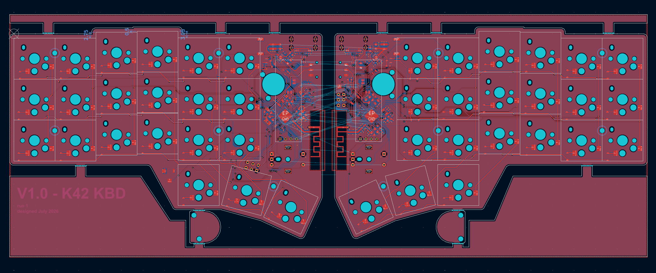
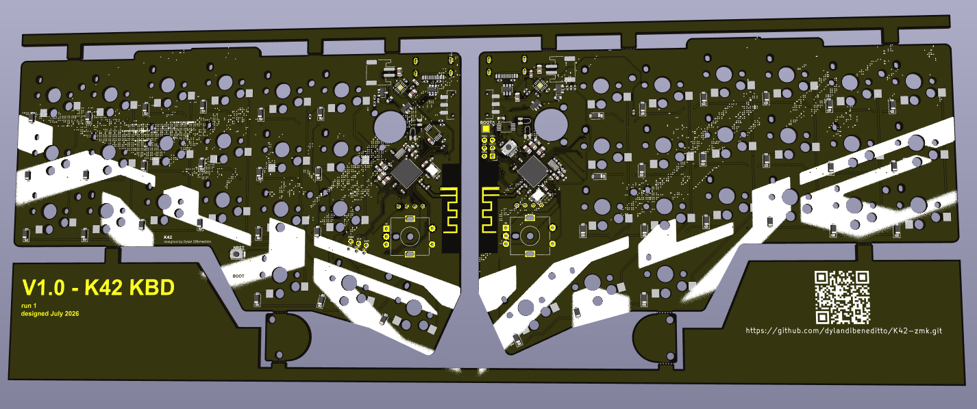
K42 is an open-source printed circuit board by dylandibeneditto, from the dylandibeneditto/k42 repository on GitHub. It is a 2-layer board of 145.2 × 98.4 mm with 117 parts on 55 nets, routed with 805 tracks and 107 vias.
It is built around the DRV2605LDGS and 1N4148W. Its parts include 45 switches, 42 diodes, 4 ICs, 2 connectors and 1 capacitor. It belongs with the keyboards and input boards of this library.
One prototype for me cost ~$250, so buying the kit saves a significant amount
| Qty | Value | Footprint | References |
|---|---|---|---|
| 42 | 1N4148W | Diode_SMD:D_SOD-123 | D1, D1, D10, D10, D11, D11, D12, D12, D13, D13, D14, D14, D15, D15, D16, D16 +26 |
| 42 | SW_Push | kbd:keyswitch_choc12_hotswap_1u | SW1, SW1, SW10, SW10, SW11, SW11, SW12, SW12, SW13, SW13, SW14, SW14, SW15, SW15, SW16, SW16 +26 |
| 12 | SolderJumper_2_Open | Jumper:SolderJumper-2_P1.3mm_Open_TrianglePad1.0x1.5mm | JP1, JP2, JP3, JP4, JP5, JP6, JP7, JP8, JP9, JP10, JP11, JP12 |
| 5 | MountingHole | MountingHole:MountingHole_2.2mm_M2_Pad | H1, H2, H4, H5, H7 |
| 4 | MountingHole | MountingHole:MountingHole_2.2mm_M2 | H3, H3, H6, H6 |
| 2 | DRV2605LDGS | Package_SO:TSSOP-10_3x3mm_P0.5mm | U1, U1 |
| 2 | SW_SPDT | Button_Switch_SMD:SW_SPDT_PCM12 | SW23, SW23 |
| 1 | 1uF | Capacitor_THT:C_Disc_D7.5mm_W4.4mm_P5.00mm | C1 |
| 1 | Conn_01x02_Pin | Connector_JST:JST_PH_S2B-PH-K_1x02_P2.00mm_Horizontal | J2 |
| 1 | Conn_Haptic_LRA | Connector_PinHeader_2.54mm:PinHeader_1x02_P2.54mm_Vertical | J1 |
| 1 | RotaryEncoder_Switch_MP | Rotary_Encoder:RotaryEncoder_Alps_EC11E-Switch_Vertical_H20mm_MountingHoles | SW22 |
| 1 | ~ | footprints:nrf52840 | U3 |
| 1 | ~ | Connector_PinHeader_2.54mm:PinHeader_1x04_P2.54mm_Vertical | U2 |
The 115 most common of 117 parts.

KOEGlike/meko
A linux music player with ddr3, a 70hz e-paper display and a haptic touchpad

sffubs/dactyl_manuform_gimbal
Instrutions and designs for building the dactyl-manuform-gimbal keyboard

sandgum/Triangulate-ES_01-Watch
A 5mm thick smartwatch which uses an E-ink display and two OLEDs to display information while consuming very little power


brendena/Nordic_Pebble_Steel
The goal of this project is to replace the main motherboard in the pebble steel with newer parts. Specifically the cpu will be a Nordic NRF52840.


ollyoid/Printegrated-Circuits
GCode post-processor for integrating PCBs into 3D prints
It measures 145.2 × 98.4 mm and has 2 copper layers, 1.6 mm thick.
117 parts, built around the DRV2605LDGS and 1N4148W. The full list of its parts is on this page, with links to each part's symbol and footprint where PCBKit's library has them.
From the dylandibeneditto/k42 repository on GitHub, at the commit this page was made from: the board is pcb/pcb.kicad_pcb and its schematic pcb/pcb.kicad_sch. PCBKit opens the board in the browser, with nothing to install.
Its repository states no licence, so its author keeps all rights: ask dylandibeneditto before reusing the design.