
2 layers333.4 × 149.9 mm
 dvallemo/7555-Timer-PCB
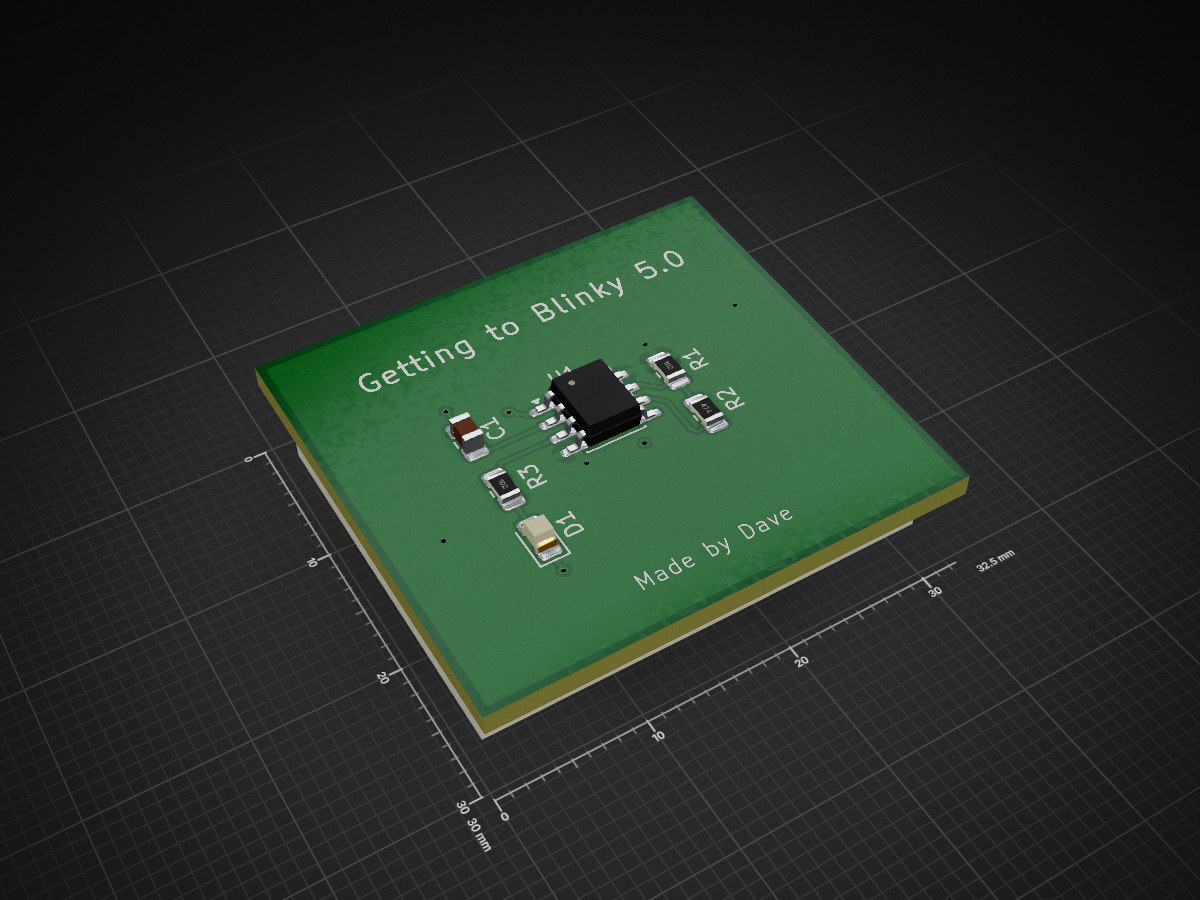
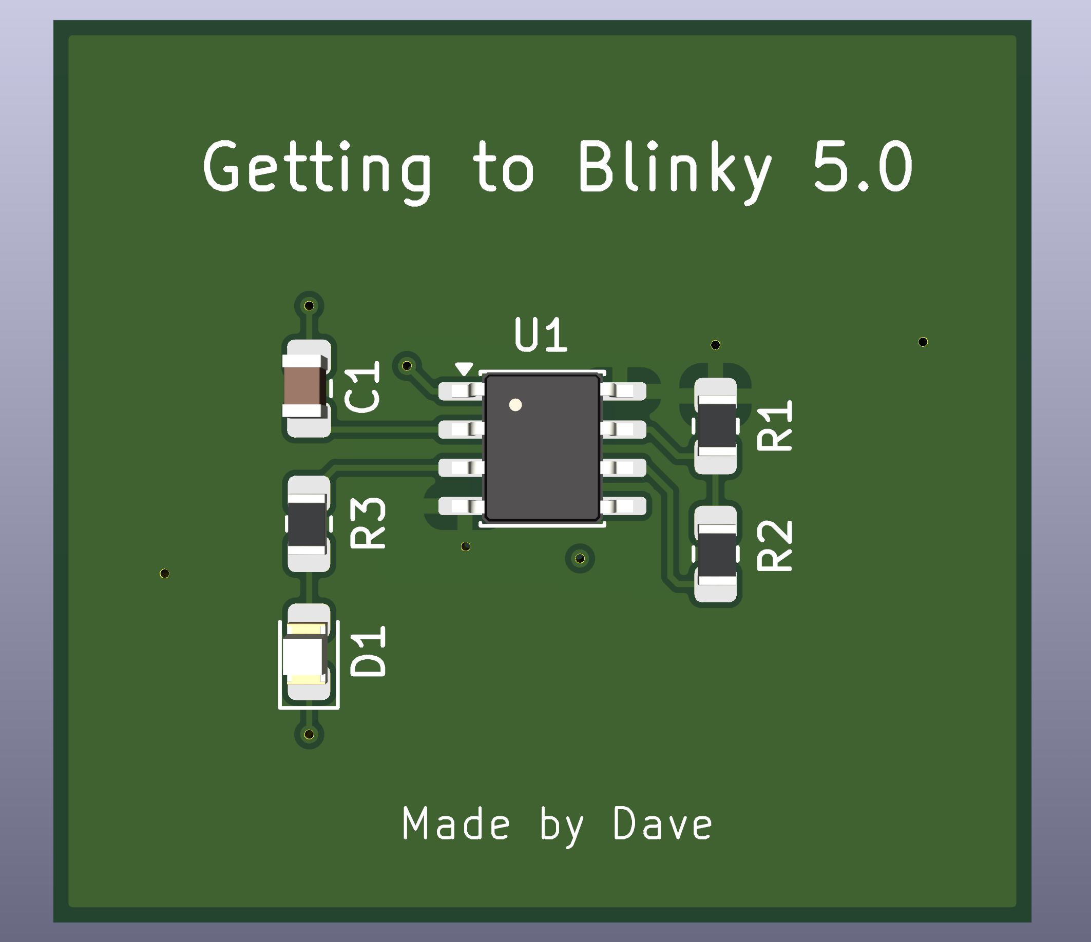
A two-layer PCB designed in KiCad featuring a 7555 CMOS timer astable oscillator circuit that blinks an LED. Built as a hands-on learning project to develop familiarity with KiCad schematic capture, footprint assignment, PCB layout, and DRC workflow.
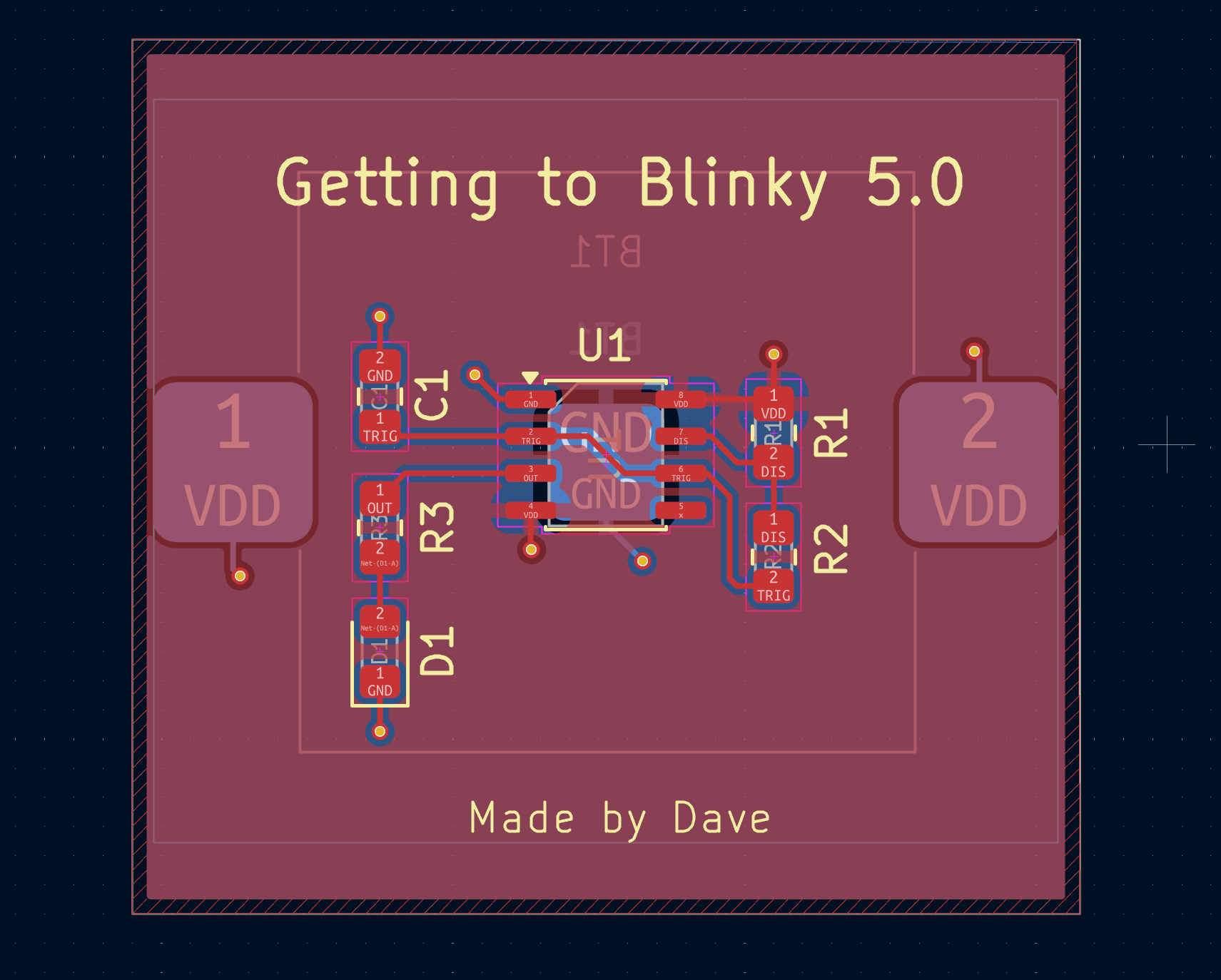
FlashLED is an open-source printed circuit board by dvallemo, from the dvallemo/7555-Timer-PCB repository on GitHub. It is a 2-layer board of 32.5 × 30 mm with 7 parts on 7 nets, routed with 32 tracks and 8 vias.
It is built around the CR2032. Its parts include 3 resistors, 1 capacitor, 1 IC and 1 diode.
A two-layer PCB designed in KiCad featuring a 7555 CMOS timer astable oscillator circuit that blinks an LED. Built as a hands-on learning project to develop familiarity with KiCad schematic capture, footprint assignment, PCB layout, and DRC workflow.
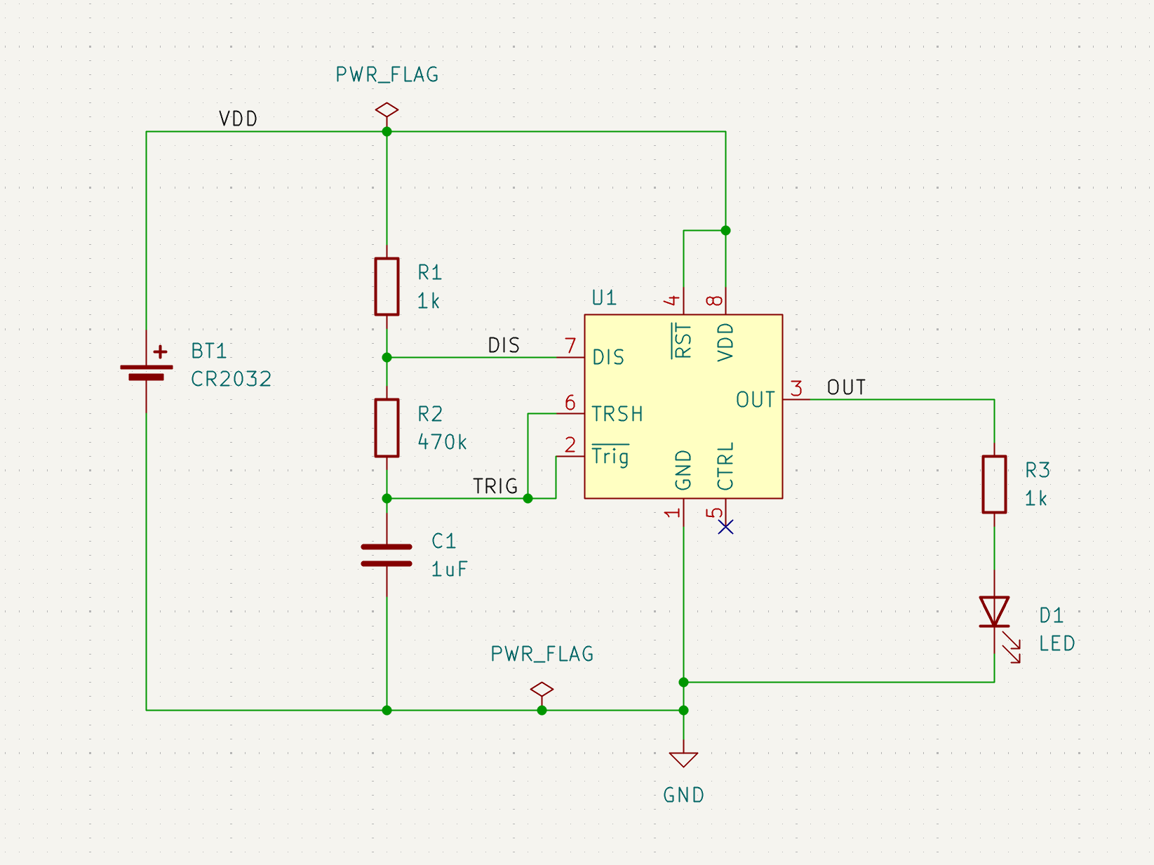
The circuit uses a 7555 timer (U1) configured in astable mode to generate a continuous square wave output that drives an LED.
| Ref | Part | Value | Description |
|---|---|---|---|
| U1 | 7555 Timer | - | SO-8 SMD package, custom schematic symbol |
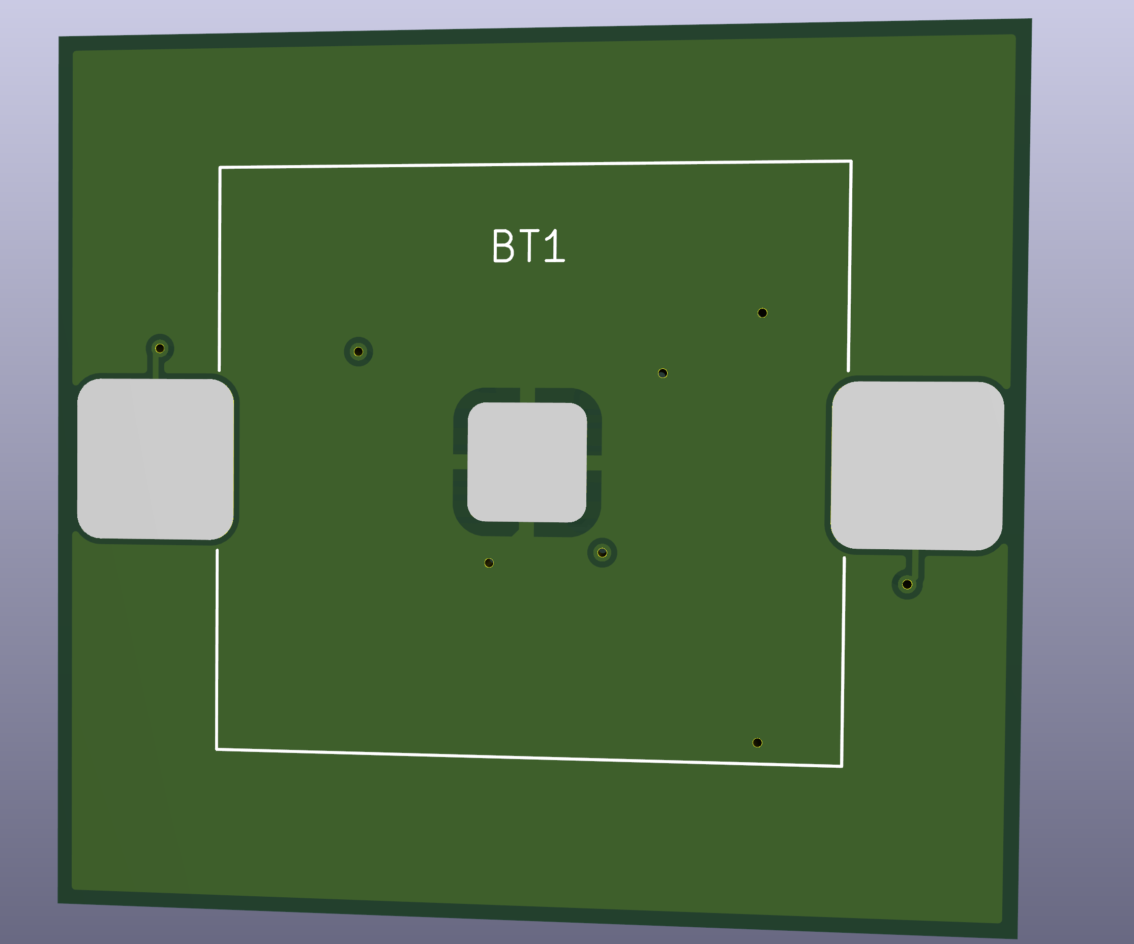
| BT1 | CR2032 | 3V | Coin cell battery, custom PCB footprint |
| R1 | Resistor | 1k ohm | Timing resistor (charge path) |
| R2 | Resistor | 470k ohm | Timing resistor (discharge path) |
| R3 | Resistor | 1k ohm | LED current limiting resistor |
| C1 | Capacitor | 1uF | Timing capacitor |
| D1 | LED | - | Output indicator, 0805 SMD |
The 7555 timer alternately charges and discharges C1 through R1 and R2, producing a square wave on the OUT pin (pin 3). R3 limits current through D1. The blink frequency is approximately:
f = 1.44 / ((R1 + 2*R2) * C1)
f = 1.44 / ((1k + 2*470k) * 1uF) = 1.53 Hz| Category | Count |
|---|---|
| Errors | 0 |
| Warnings | 4 |
| Unconnected Items | 0 |
The 4 warnings are non-critical: 3 are single-layer via warnings resolved after copper pour fill, and 1 is a footprint-library mismatch on BT1 due to the custom footprint.
Dave - Electrical Engineering, Stevens Institute of Technology
PCB design portfolio project | KiCad | June 2026
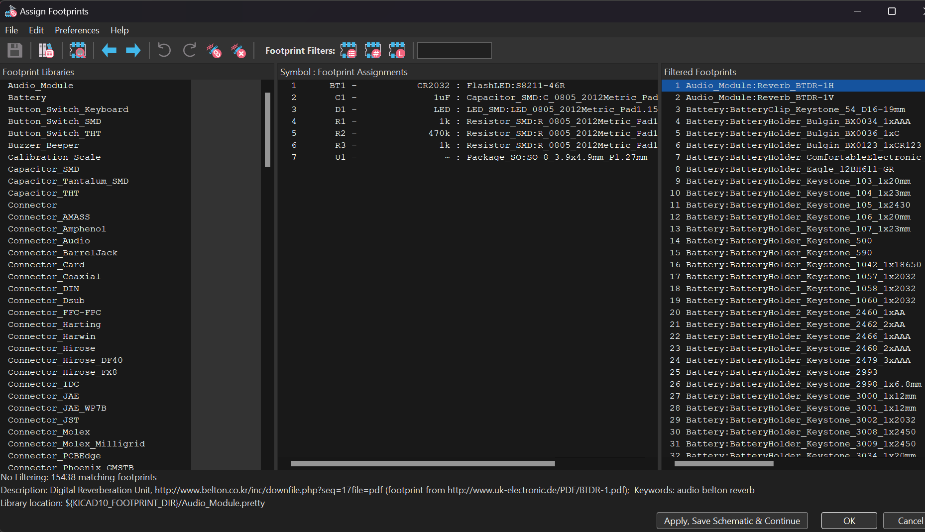
| Qty | Value | Footprint | References |
|---|---|---|---|
| 2 | 1k | Resistor_SMD:R_0805_2012Metric_Pad1.20x1.40mm_HandSolder | R1, R3 |
| 1 | 1uF | Capacitor_SMD:C_0805_2012Metric_Pad1.18x1.45mm_HandSolder | C1 |
| 1 | 470k | Resistor_SMD:R_0805_2012Metric_Pad1.20x1.40mm_HandSolder | R2 |
| 1 | CR2032 | FlashLED:S8211-46R | BT1 |
| 1 | LED | LED_SMD:LED_0805_2012Metric_Pad1.15x1.40mm_HandSolder | D1 |
| 1 | ~ | Package_SO:SO-8_3.9x4.9mm_P1.27mm | U1 |
It measures 32.5 × 30 mm and has 2 copper layers, 1.6 mm thick.
7 parts, built around the CR2032. The full list of its parts is on this page, with links to each part's symbol and footprint where PCBKit's library has them.
From the dvallemo/7555-Timer-PCB repository on GitHub, at the commit this page was made from: the board is FlashLED.kicad_pcb and its schematic FlashLED.kicad_sch. PCBKit opens the board in the browser, with nothing to install.
Its repository states no licence, so its author keeps all rights: ask dvallemo before reusing the design.


skiselev/zeta_sbc
Zeta SBC is an Zilog Z80 based single board computer. It is inspired by Ampro Little Board Z80 and N8VEM project. Zeta SBC is software compatible with RomWBW Firmware