2 layers58.4 × 21.6 mm

 smaroukis/usb-sleuth61
USB cable continuity tester ++
38-04-usb sleuth is an open-source printed circuit board by smaroukis, from the smaroukis/usb-sleuth repository on GitHub. It is a 2-layer board of 90 × 89.4 mm with 68 parts on 90 nets, routed with 978 tracks and 131 vias.
It is built around the STM32C031K6T6, CR2032 and ZX-1.27BM-4PSMD. Its parts include 25 diodes, 6 connectors, 5 capacitors, 5 resistors and 2 switches. It belongs with the STM32 boards of this library.


See this README for usage of the STM32CubeIDE to flash firmware on the device.
The device tests for continuity and internal resistors within various USB Cables and exposes some pins for multimeter testing. The project is a hardware fork of aroerina/LimePulse that I decided to reverse engineer and write the firmware for.
A STM32C031K6T microcontroller is used for testing connection and orientation, powered by a CR2032 battery. Code is given using STM32 HAL libraries and the device can being programmed over SWD.
KiCad and gerber files are provided for the board layout, as well as the library footprints for non-standard parts ordered from JLCPCB/LCSC. See the BOM.
This USB cable tester has the "B" side on the right, and the "A" side on the left. Receptacles are given for the following:
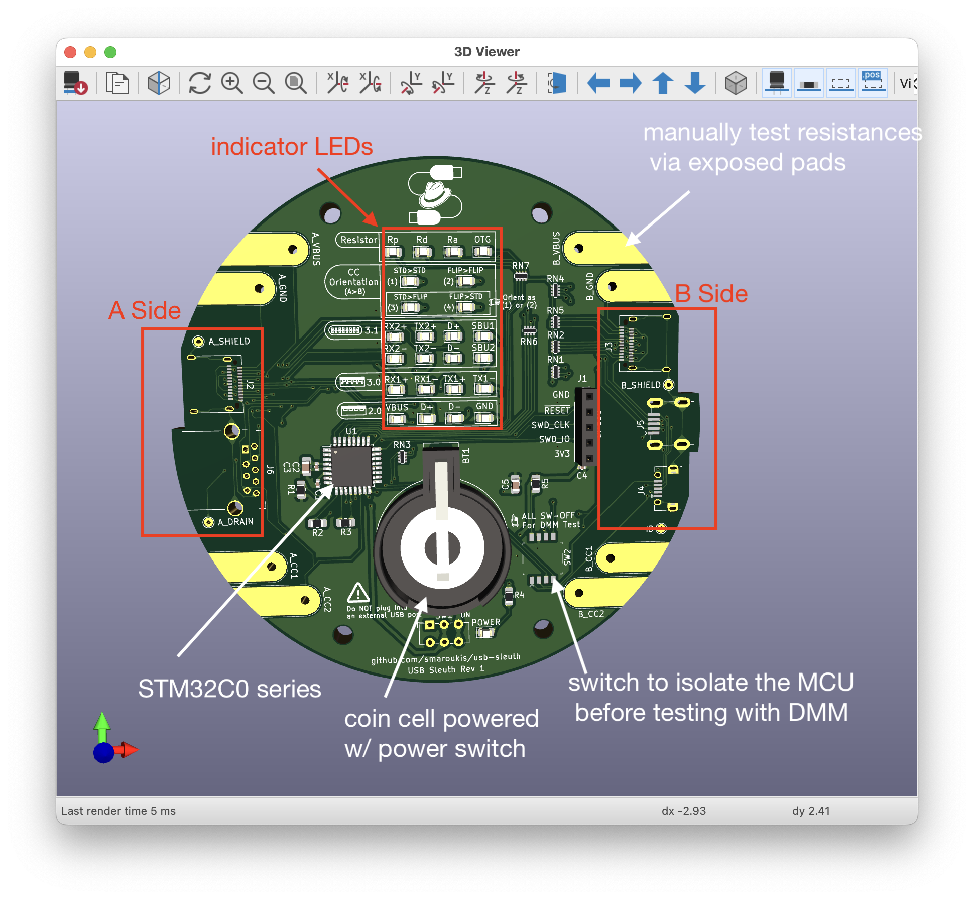
The device has some benefits over a simple continuity tester
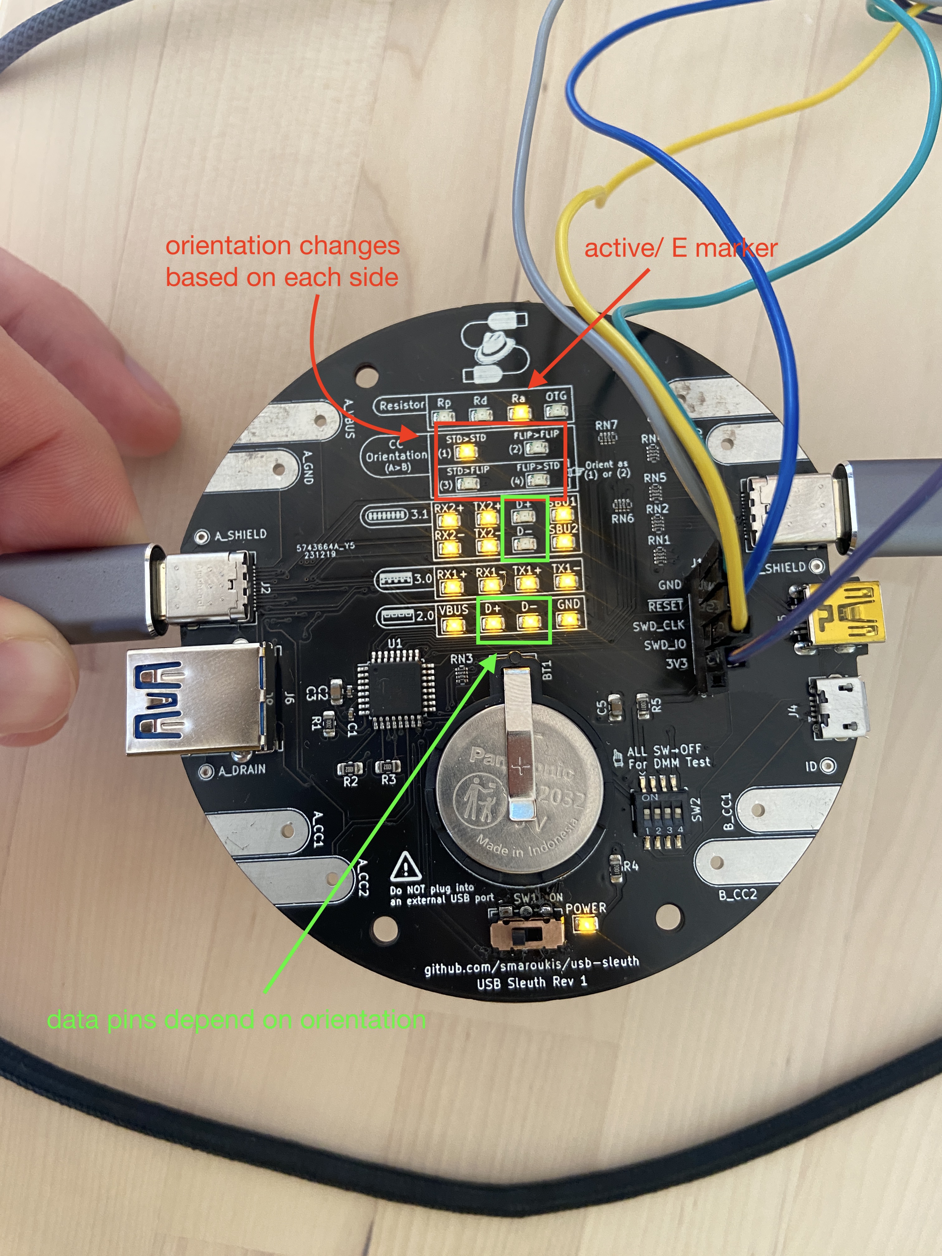
Note in this test only one of the USB 2.0 Data pair LEDs will light up depending on the cable orientation, showing that the two pairs are not connected inside the cable (the pairs are also not connected on the PCB). The user must flip the orientation to test both data pairs.
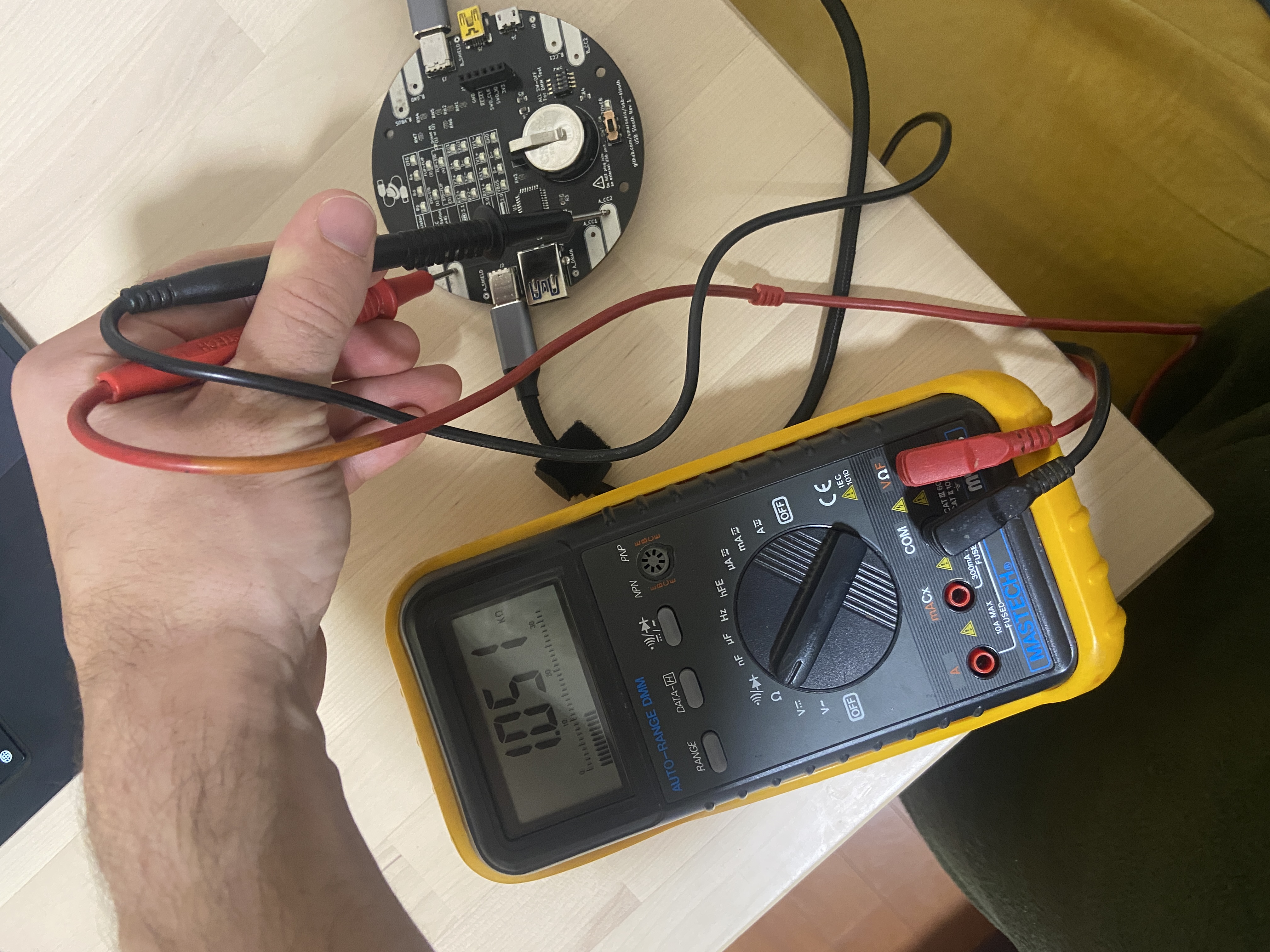
Testing the value of the pulldown resistor on an active cable by measuring between B_CC2 and B_GND (should be between 800-1.2K Ohms).
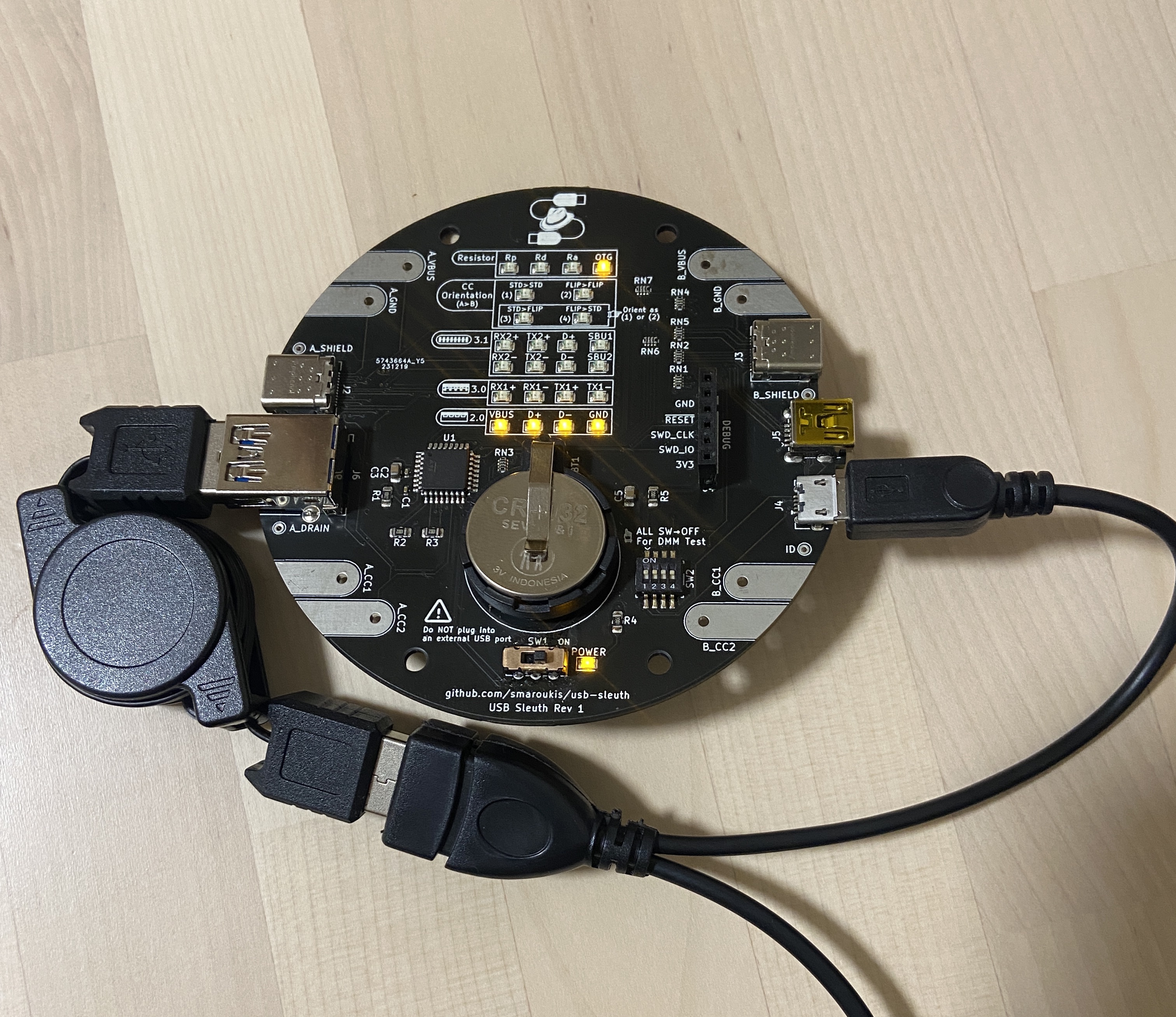
Layout
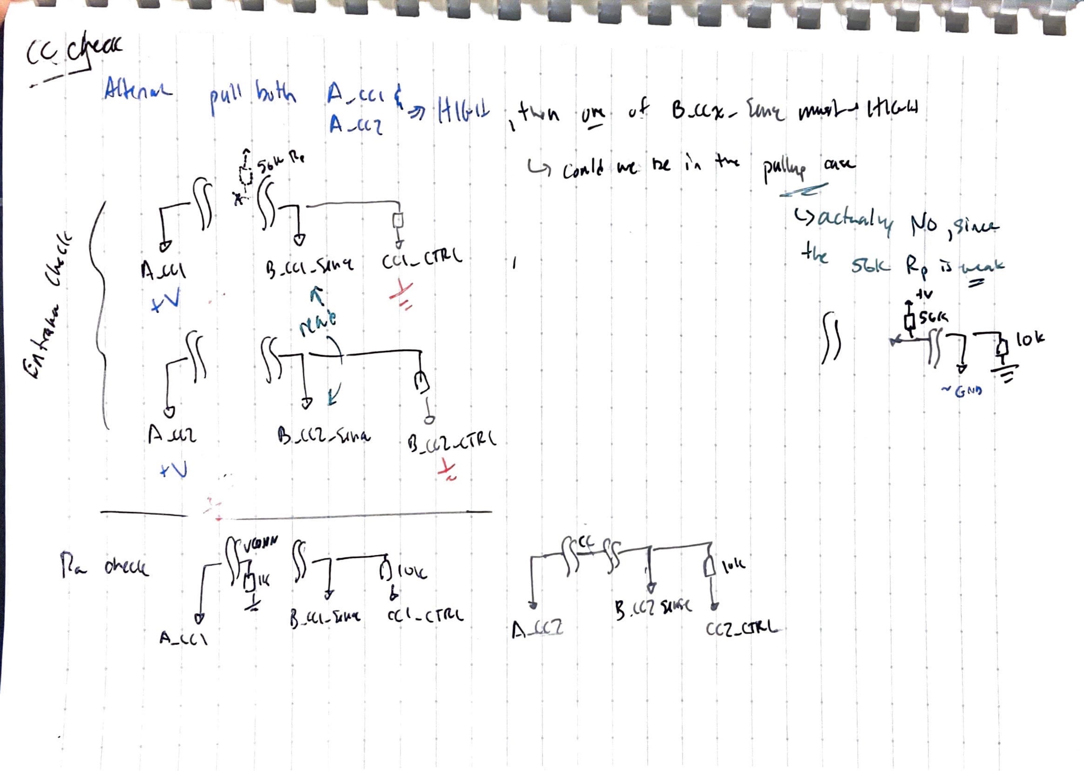
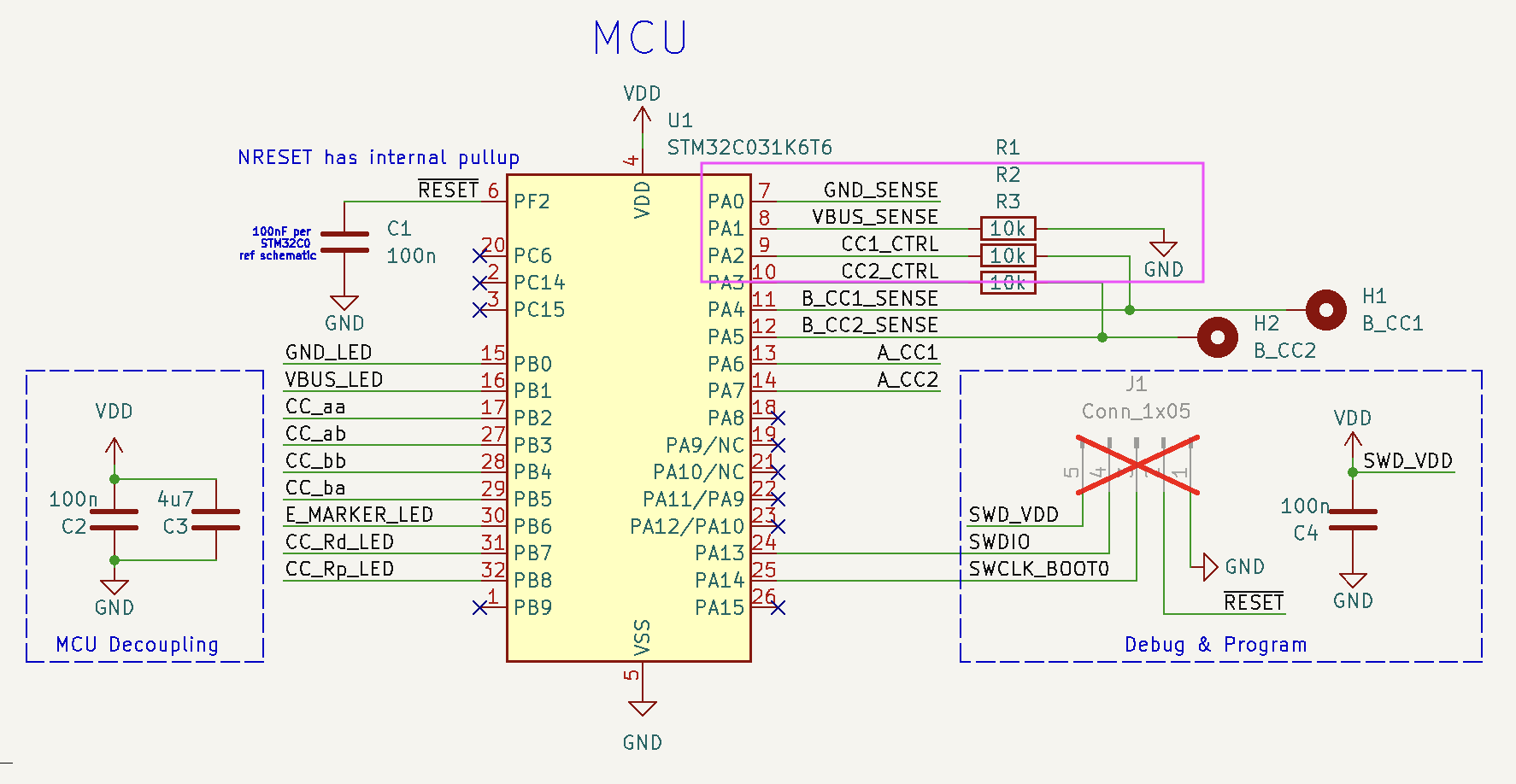
Note: Both A-side and B-side CC1 and CC2 pins are tapped off into corresponding control inputs to the MCU through a resistor, allowing for pulling the control pins high or low to sense the result on the opposite side.
Simplified layout of testing CC1 pin.
Programming is done via the Serial Wire Debug headers (labeled DEBUG) via an STLink debugger probe.
The device can also be reset by shorting out the nRESET line to GND (pins 1 and 2 on the header).
[!CAUTION] In the case where the debugger is providing power to the target, make sure the
POWERswitch isOFF.
[!NOTE] For the
SWDpins we need pullup or pulldown resistors onSWDIOandSDCLKrespectively. These are provided internally by the STM32 MCU, but if there is an issue with the debugger try adding an external weak pulllup and pulldown (10K-100K).
[!NOTE]
VBUS: Pulled up on B-side to VDD via 2K, pulled down to ground at A-side MCU input sense pin via 10K. Sense pin reads high if VBUS line is continuous through the cable.GND: B-side receptacle ground pin connected to board ground, A-side receptacle pin is direct to input sense pin.
All VBUS pins are tied together and tested via a pulldown resistor on the MCU (similarly for GND pins).
Most B-side receptacle pins are pulled up to supply/VDD through resistors with exception for CC pins and Ground. B-side ground is connected to board ground through a DIP switch for isolation from the MCU ground if needed.
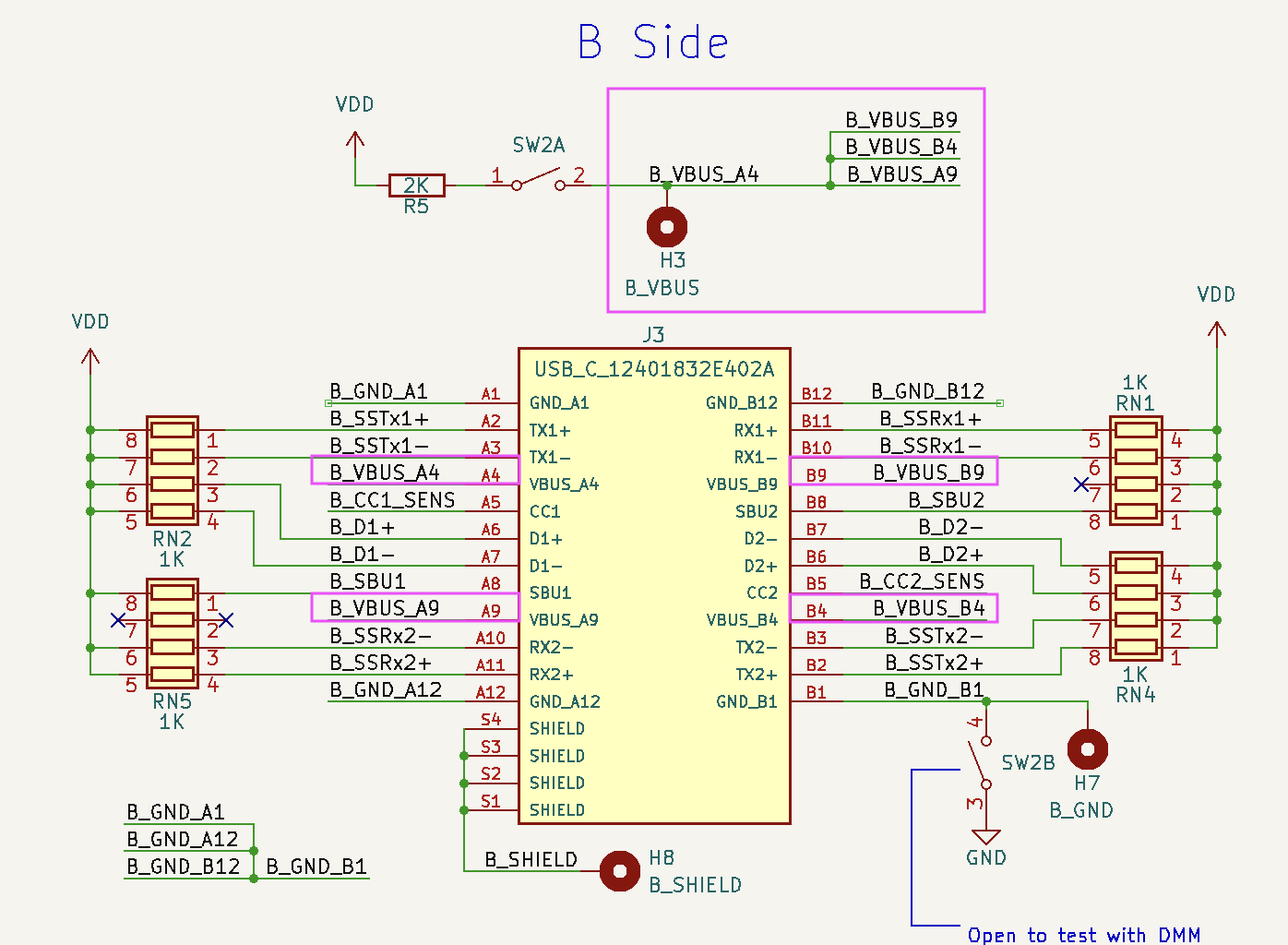
A-side receptacle pins are connected to the MCU input for sensing.
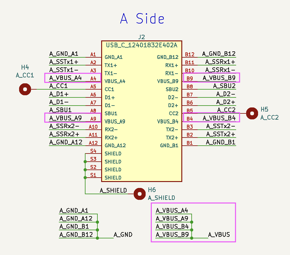
A_VBUS/A_GND and connected to VBUS_SENSE/GND_SENSE inputs to the MCU through DIP switches for isolation from the MCU during DMM testing.
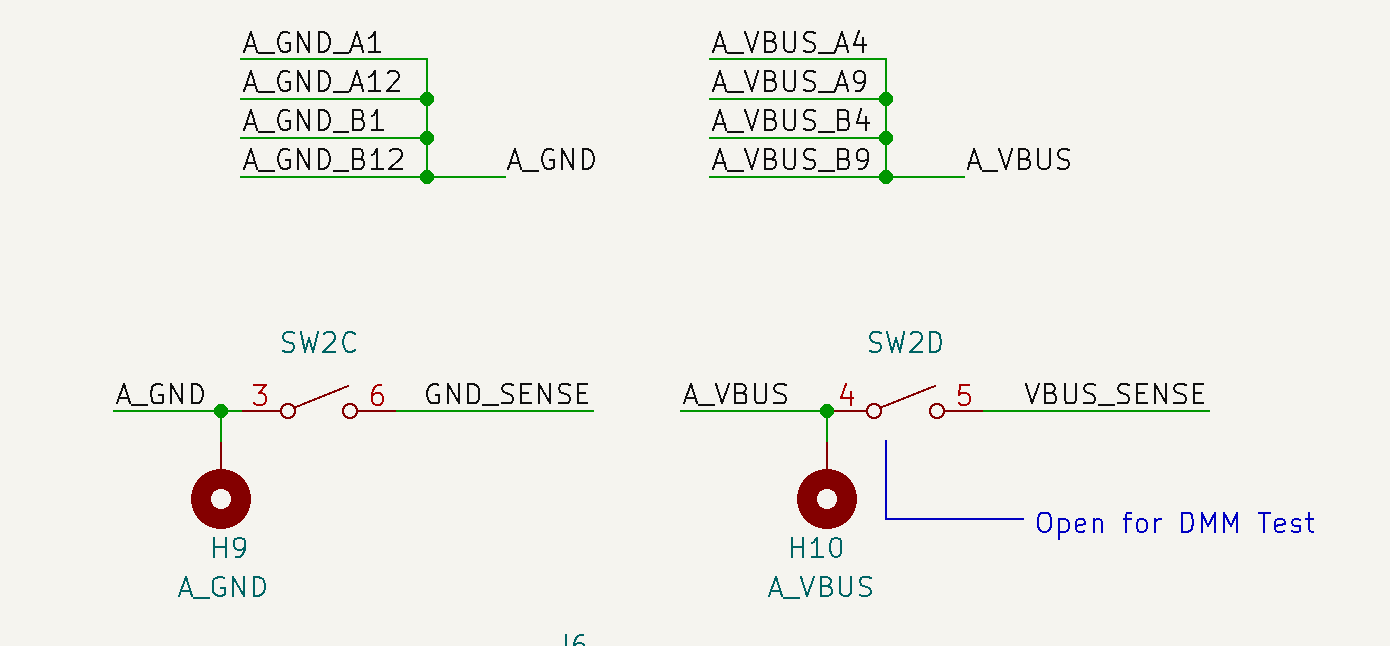
VBUS_SENSE pin is an input to the MCU with a pull down resistor forming a voltage divider with the 2K VDD pulllup resistor. If the VBUS line is discontinuous, the pin reads LOW. If VBUS is continuous then the pin reads VCCx10/12, or digital HIGH.
Indicator LEDs are driven by the MCU outputs GND_LED and VBUS_LED.
Here is the type-C receptacle pinout
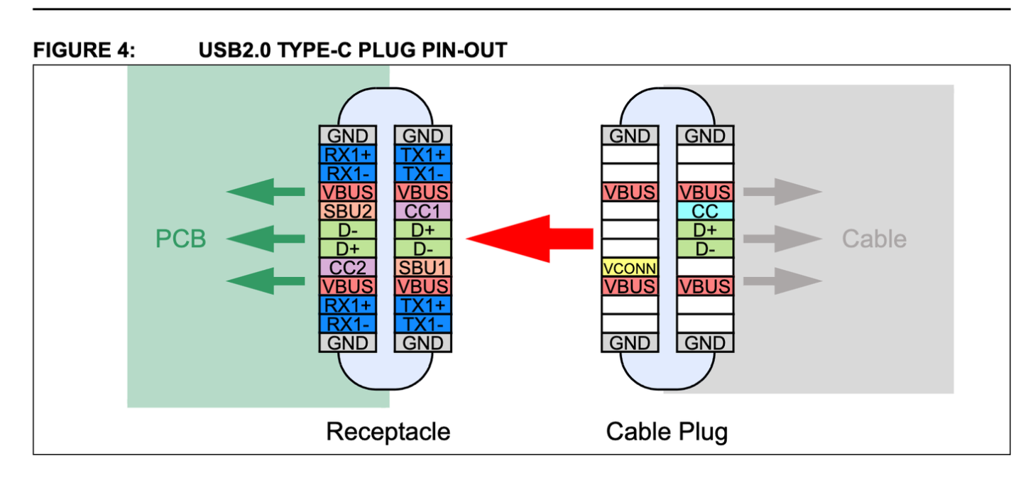
Source: "USB 2.0 Type-C Plug Pin-Out" https://ww1.microchip.com/downloads/en/appnotes/00001953a.pdf
Possible orientations of USB-C Plug.
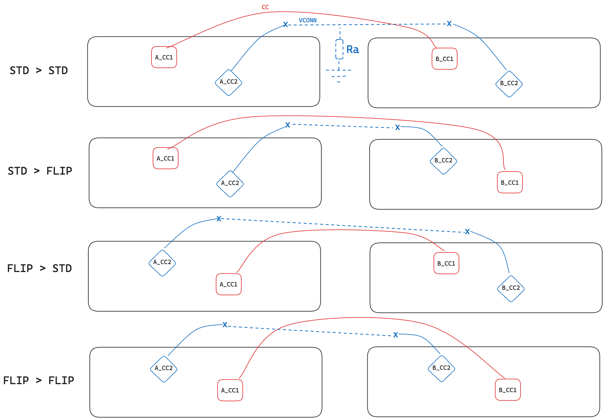
Note Ra is for the active pulldown emarker, but don't take this "straight through" configuration literally as there are diodes preventing shorting of the pins.
Simplified PCB layout:
We can determine that a C-C type cable is connected by pulling both A_CC1 and A_CC2 HIGH and CCx_CTRL pins LOW, then looking for one of the B_CCx pins coming HIGH.
The pulldown (Ra, for "active") is nominally 800-1.2K. Connection is as follows:
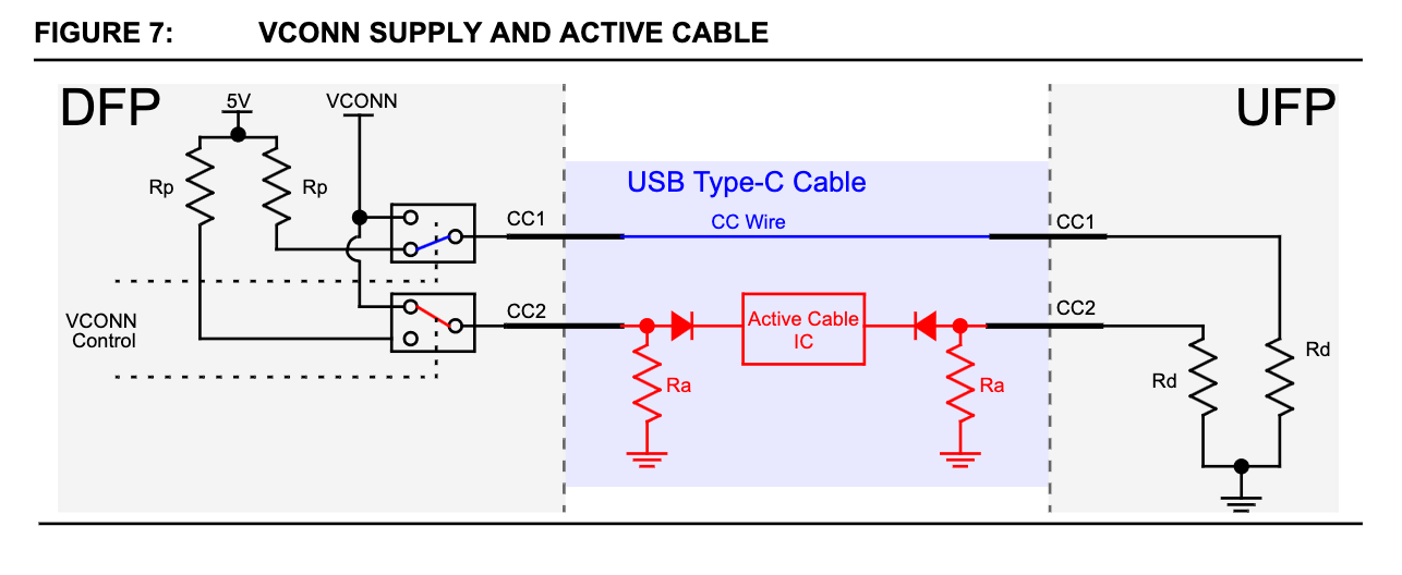
We simply configure the A_CC2 and B_CC2 pins as INPUT_PULLUPs and test if these lines (the VCONN line) are pulled low (normally it is open), since the pulldown Ra is strong at ~1K.
[!NOTE] It is programmed to work for both USB-C plug orientations
Setup
VBUS is connected to VCC through a 2K resistor (ignored for the calculations below)CC1_CTRL and CC2_CTRL → LOW (pulls B_CCx pin toward ground through 10K R)B_CC1_sense and B_CC2_SENSERP_THRESH, to account for ground noise, then the 56K Rp pullup exists.[!TIP] An analog read is required since the internal Rp is weak enough such that it doesn't pull it all the way up to the digital
HIGHthreshold
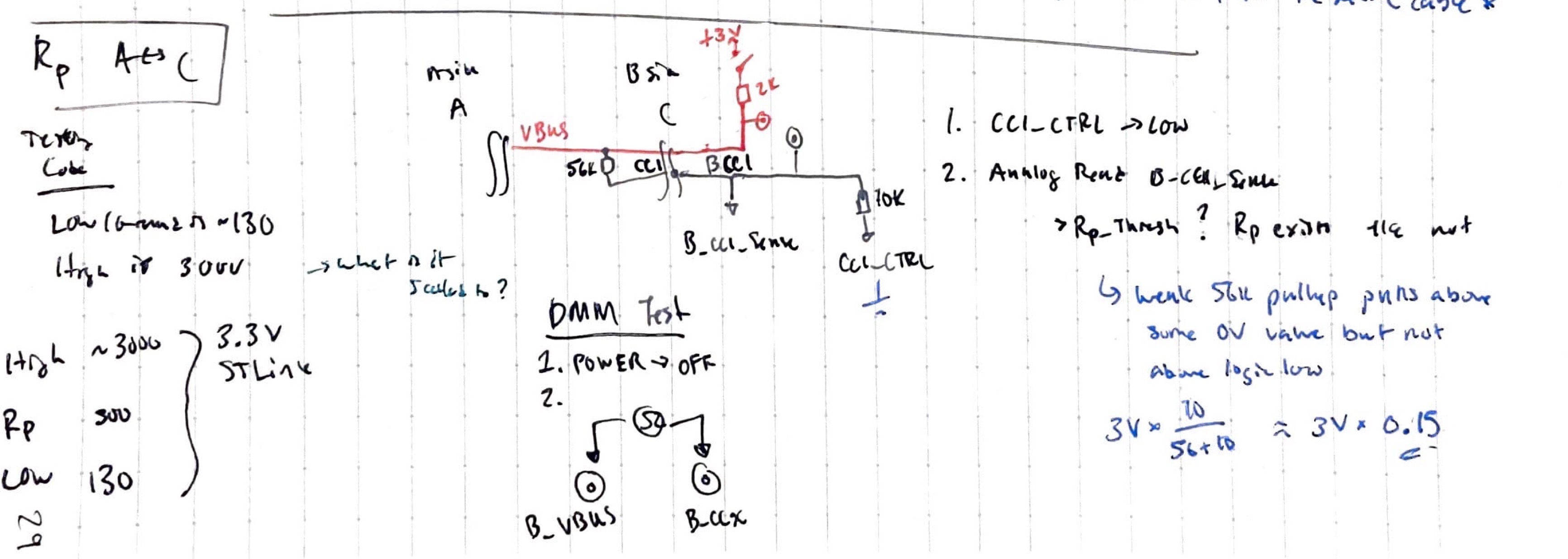
Note this works for both CC configurations
A_CC1 as INPUT_PULLUP (~50K internal pullup)A_CC1, if pulled LOW, then it means that Rp is present (Rd = 5K which is much stronger than the 50K internal pullup)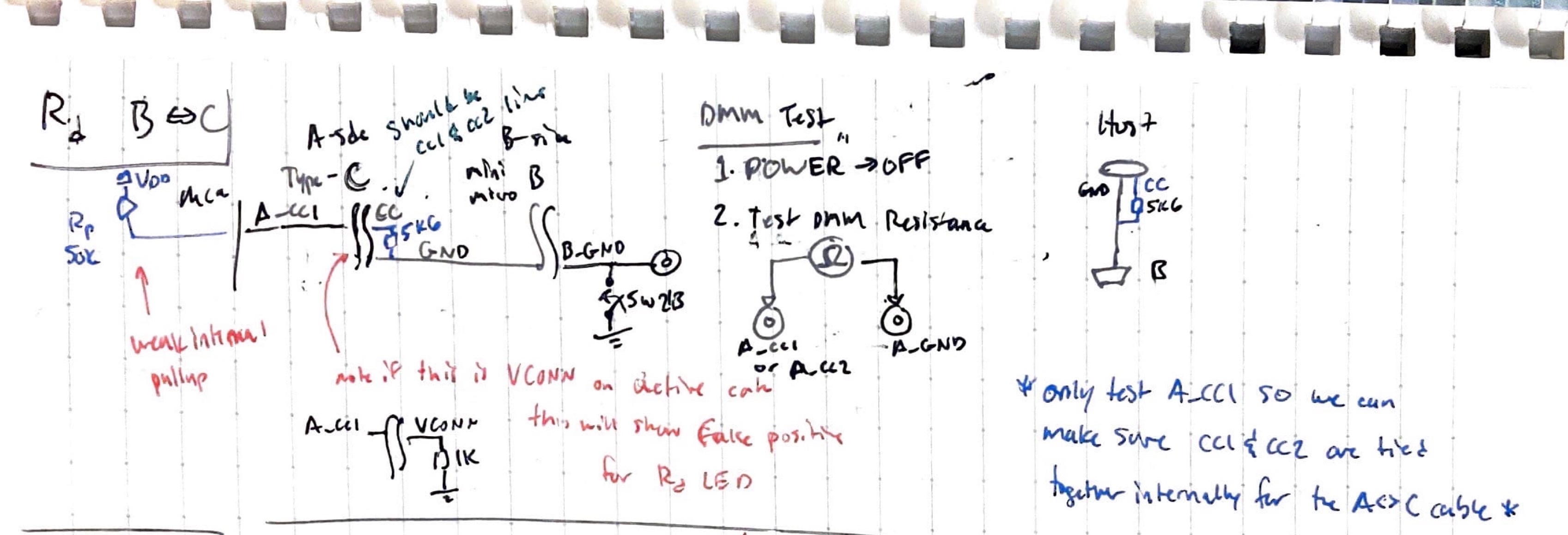
Isolation switches are provided to isolate the DMM from the MCU as it injects a test current to measure resistance, and also to allow us to measure the resistance of the cable itself (e.g. VBUS to GND).
Note during testing it was found that even with the switches closed the DMM measurements weren't affected.
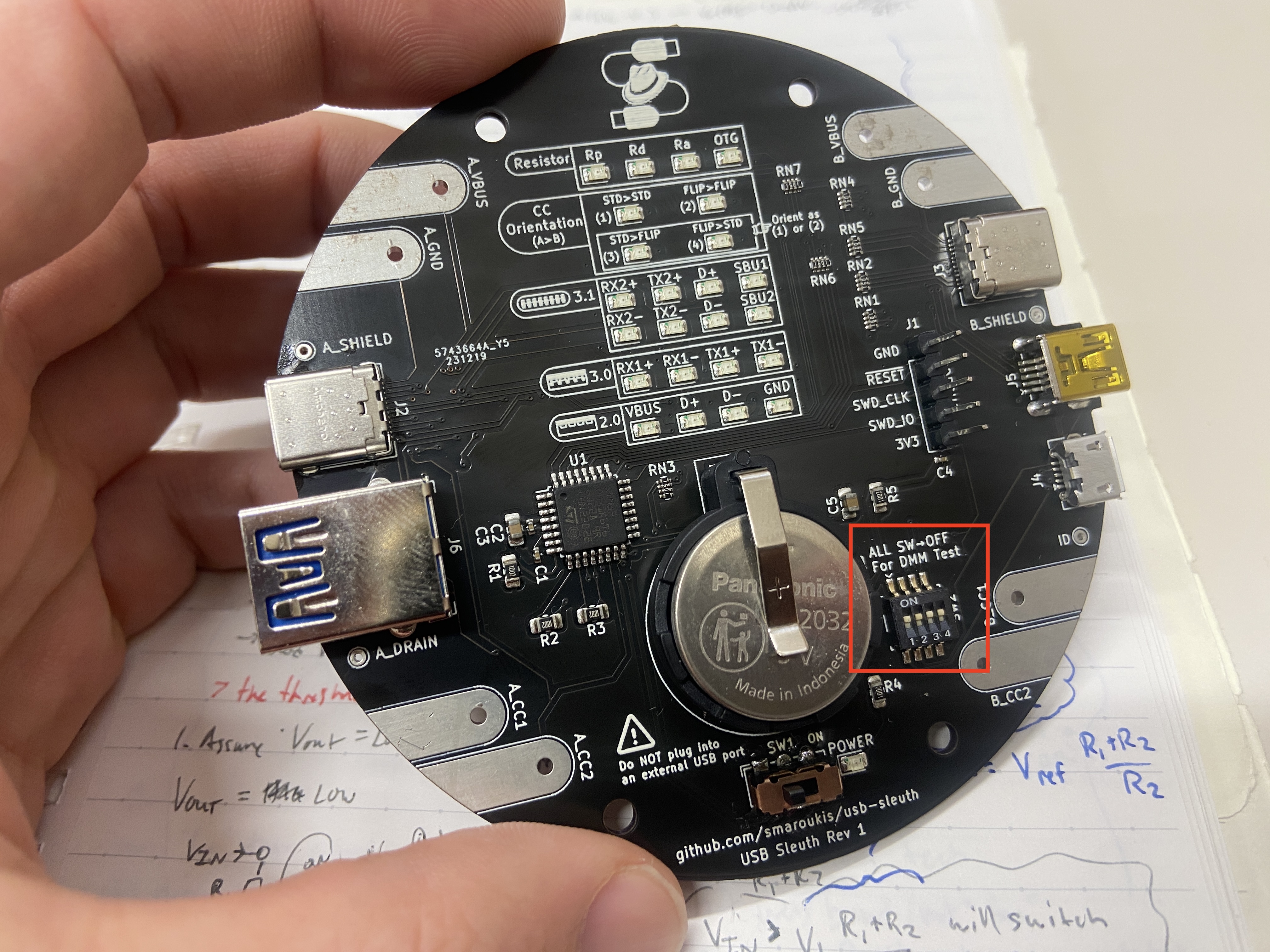
In the schematic these are modeled as a multi-unit DIP switch:
SW2A: Separates VCC from VBUSSW2B: Separates B_GND from GNDSW2C: Separates A_GND from A_GND_SENSE (input to MCU)SW2D: Separates A_VBUS from A_VBUS_SENSE (input to MCU)[!Caution] Verify the following:
- USB cable is in the normal CC Orientation of
STD>STDbefore proceeding (or note the configuration to choose the correct pad to test)- All DIP switches are in the OFF position
- Power switch is in the OFF position
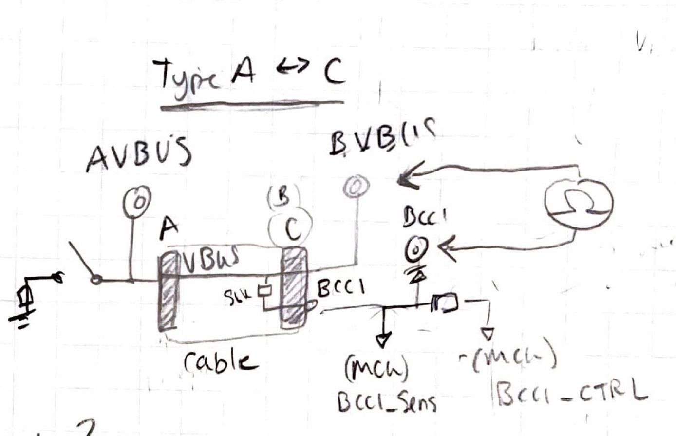
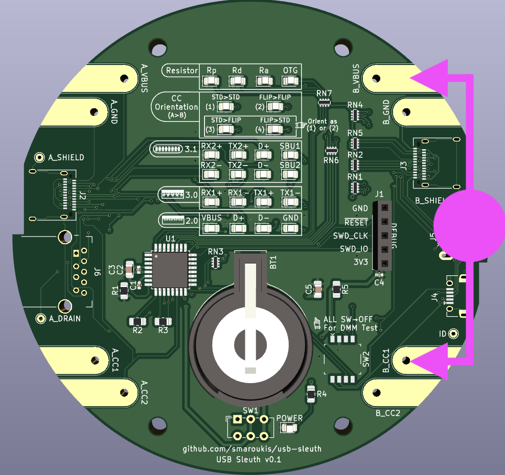
For the Type-A to C cable the USB standard specifies at 56K pullup resistor between VBUS and CC (since the A side is the host, CC pin needs to be pulled up for the B-side/peripheral to recognize A side as host).
We can test the exact value of this resistor by using a DMM between B_VBUS and B_CC1 testing pads.
[!Caution] Verify the following:
- USB cable is in the normal CC Orientation of
STD>STDbefore proceeding (or note the configuration to choose the correct pad to test)- All DIP switches are in the OFF position
- Power switch is in the OFF position
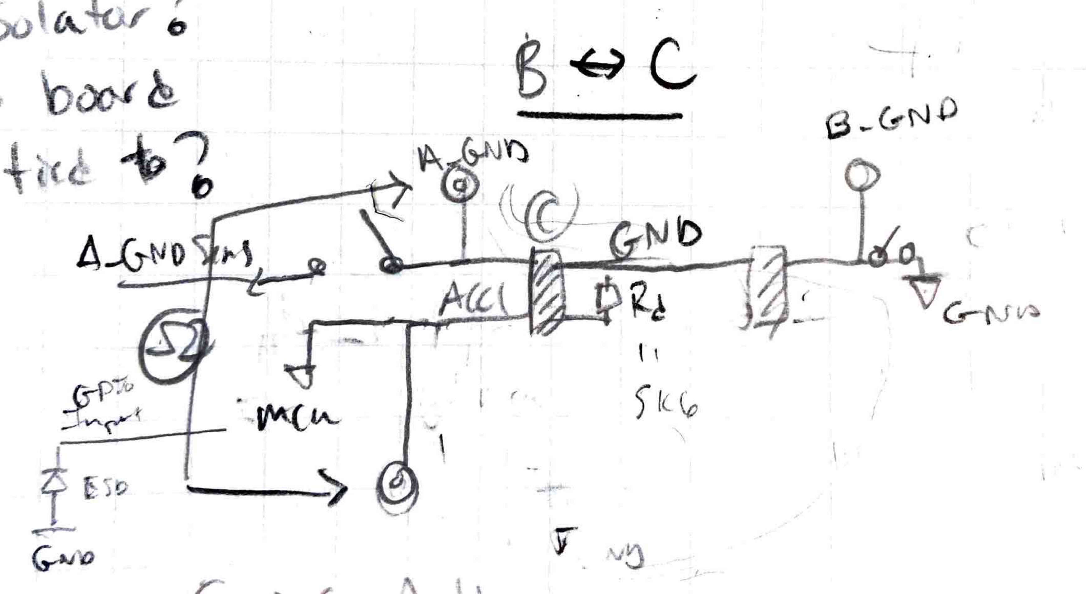
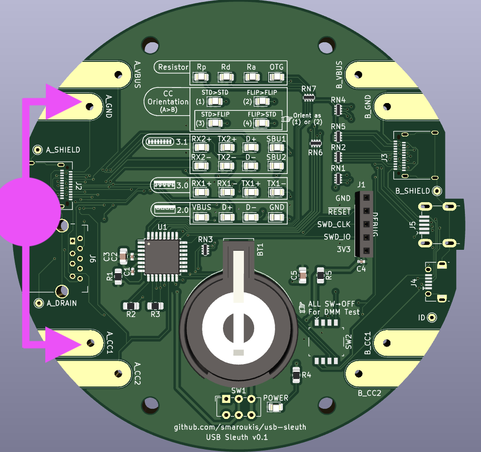
For the Type-B to C cable the USB standard specifies at 5K6 pulldown resistor between CC and GND (since the B side is the peripheral, CC pin needs to be pulled down for the A-side/host to recognize B side as peripheral).
We can test the exact value of this resistor by using a DMM between
A_GND and A_CC1
STD>STDB_CC2 and B_GND since the Ra will be on the VCONN line.Shields are connected together and exposed to a through hole testing terminal. For this we can test with a multimeter.
Note the shield and ground are connected inside the receptacle.
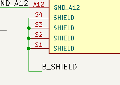
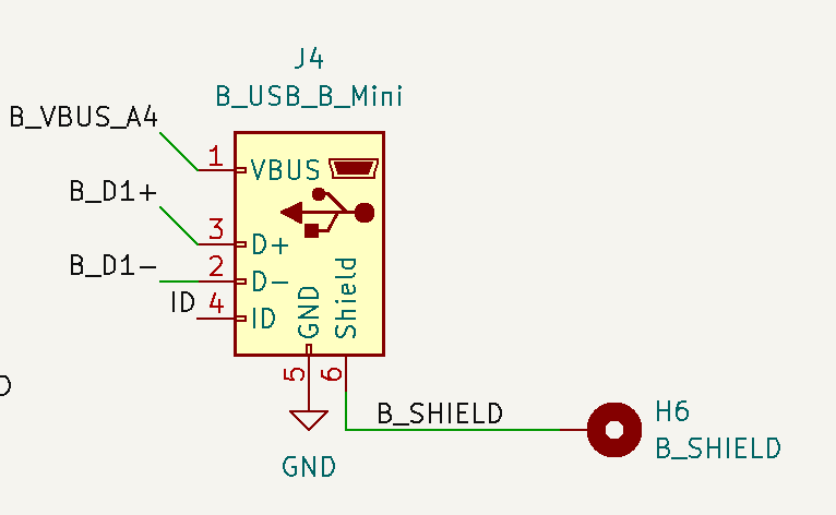
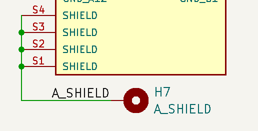
The OTG specification allows a USB device normally acting as a peripheral, to now act as a host (example use case: a tablet normally a peripheral, acting as a host can read from removable media on a flash drive)
For the OTG cable the A-plug side ties its ID pin to ground, and the B-plug side leaves it floating.
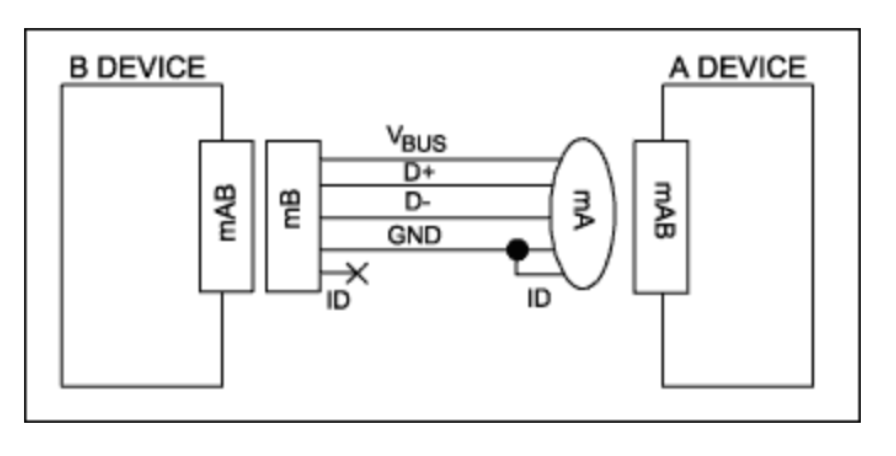
Since the ID pin is supposed to be tied to its ground pin within the plug, we just connect an LED between VDD → ID pin (=Ground pin) to test the connection.
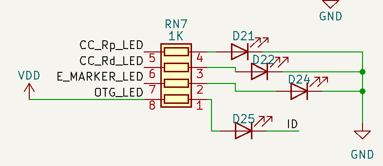
The ID pin is also brought out on an exposed pad.
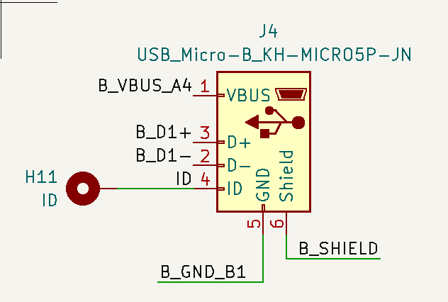
Only one set of the D+ and D- pins light up.
OTG Cable test doesn't work?
If the OTG cable has two male plugs, the data lines are not connected between the male ends, only from female → male 1 and female → male 2. The proper way to test will require the OTG adapter plus a normal USB cable.
With one end plugged in, when I touch the other cable plug to the receptacle the GND (and sometimes Rd) LEDs light up.
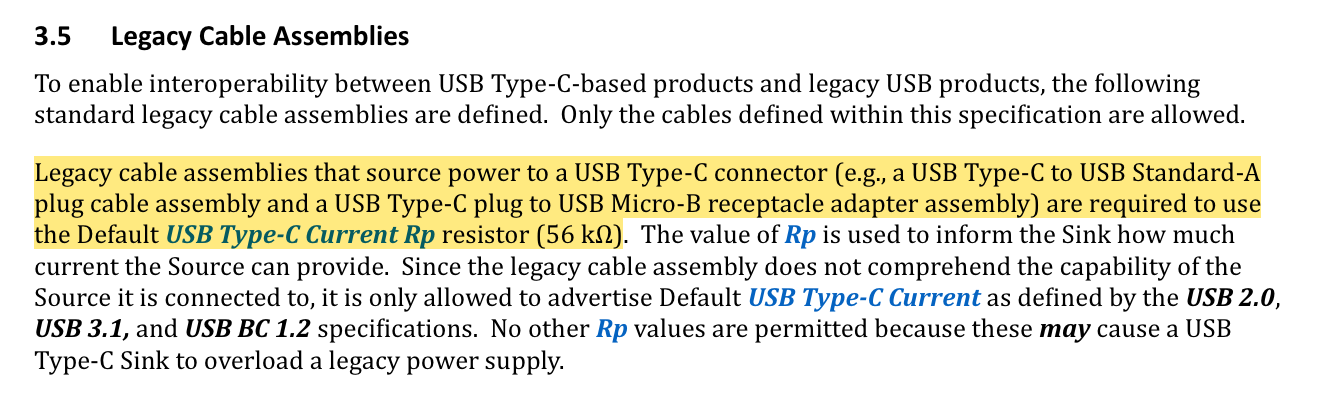
The USB-C Type Spec provides the Rp and Rd requirements for legacy cables.
For example, Type-C to 2.0 Type A:
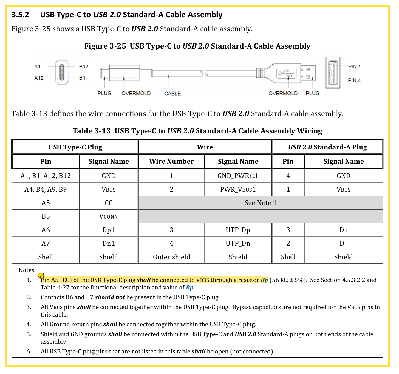
USB Type-C Spec R2.3 - October 2023.pdf
tl;dr any legacy cable assembly that sources power to a Type C connector must use the default 56K pullup (note this is for both 3.1 and 2.0 versions, since the power negotiation didn't come along until later)
Note the A5 CC pin and the B5 VCONN pin are not connected internally. This means it is up to the hardware developer to implement orientation detection on the C-receptacle side.
And here is for the Type-C to 2.0 Micro-B:
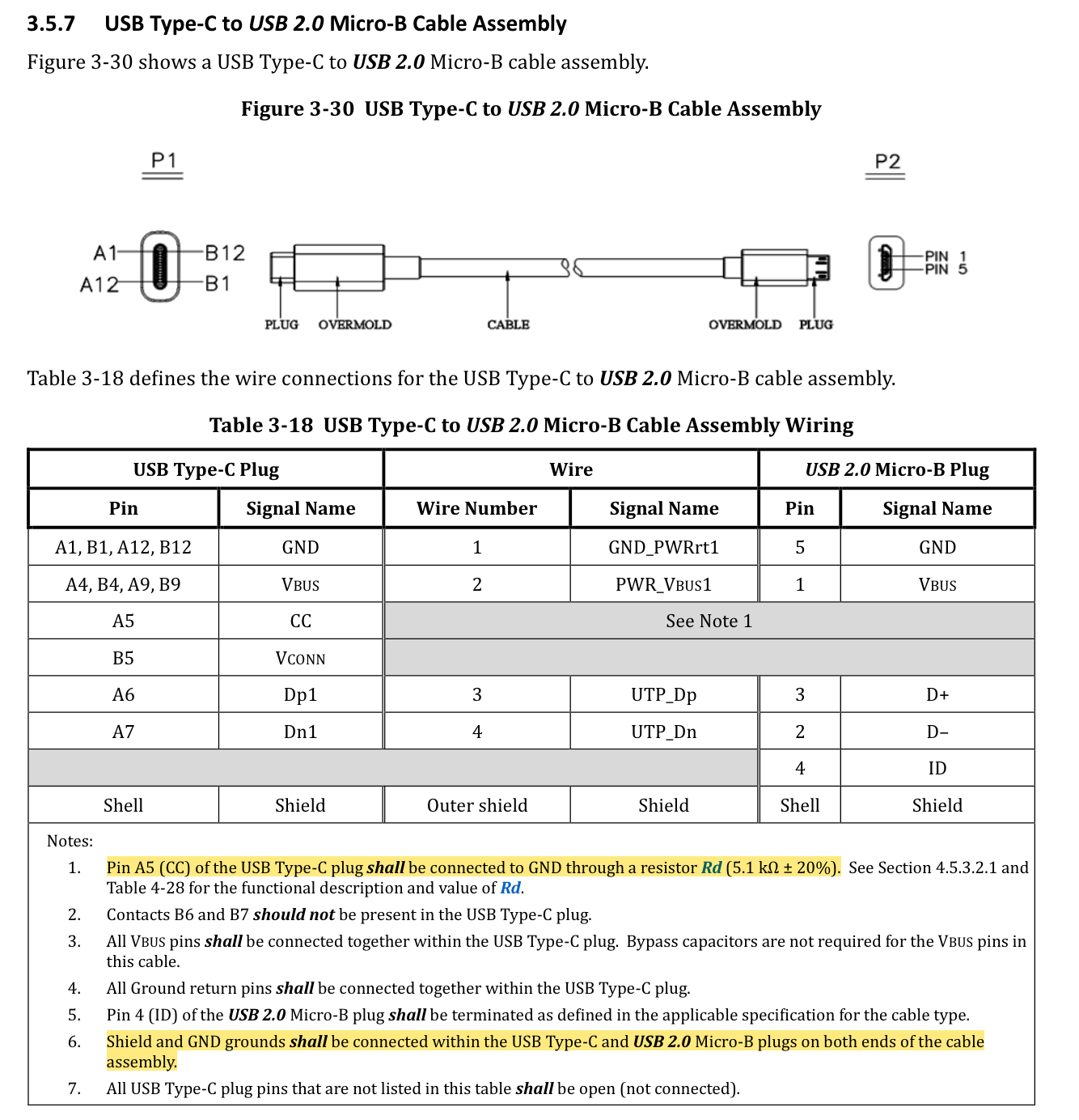 ^dzdzs5
Icons
Inspired By
| Qty | Value | Footprint | References |
|---|---|---|---|
| 25 | YLW | LED_SMD:LED_0805_2012Metric | D1, D2, D10, D11, D12, D13, D14, D15, D16, D17, D18, D19, D20, D21, D22, D23 +9 |
| 7 | 1K6 | Resistor_SMD:R_Array_Concave_4x0402 | RN1, RN2, RN3, RN4, RN5, RN6, RN7 |
| 4 | MountingHole_3.2mm_M3_DIN965 | MountingHole:MountingHole_3.2mm_M3_DIN965 | , , , |
| 3 | 100n | Capacitor_SMD:C_0402_1005Metric | C1, C2, C4 |
| 3 | 10k | Resistor_SMD:R_0805_2012Metric_Pad1.20x1.40mm_HandSolder | R1, R2, R3 |
| 2 | 2K | Resistor_SMD:R_0805_2012Metric_Pad1.20x1.40mm_HandSolder | R4, R5 |
| 2 | USB_C_12401832E402A | 01-UserFootprints:USB_C_Receptacle_Amphenol_12401832E402A | J2, J3 |
| 1 | 1uF | Capacitor_SMD:C_0805_2012Metric_Pad1.18x1.45mm_HandSolder | C5 |
| 1 | 4u7 | Capacitor_SMD:C_0805_2012Metric_Pad1.18x1.45mm_HandSolder | C3 |
| 1 | A_CC1 | 01-UserFootprints:Connector_Pad_Edge_Oval_5mm_Extended | H4 |
| 1 | A_CC2 | 01-UserFootprints:Connector_Pad_Edge_Oval_5mm_Extended | H5 |
| 1 | A_DRAIN | TestPoint:TestPoint_THTPad_D1.5mm_Drill0.7mm | H12 |
| 1 | A_GND | 01-UserFootprints:Connector_Pad_Edge_Oval_5mm_Extended | H9 |
| 1 | A_SHIELD | TestPoint:TestPoint_THTPad_D1.5mm_Drill0.7mm | H6 |
| 1 | A_VBUS | 01-UserFootprints:Connector_Pad_Edge_Oval_5mm_Extended | H10 |
| 1 | B_CC1 | 01-UserFootprints:Connector_Pad_Edge_Oval_5mm_Extended | H1 |
| 1 | B_CC2 | 01-UserFootprints:Connector_Pad_Edge_Oval_5mm_Extended | H2 |
| 1 | B_GND | 01-UserFootprints:Connector_Pad_Edge_Oval_5mm_Extended | H7 |
| 1 | B_SHIELD | TestPoint:TestPoint_THTPad_D1.5mm_Drill0.7mm | H8 |
| 1 | B_VBUS | 01-UserFootprints:Connector_Pad_Edge_Oval_5mm_Extended | H3 |
| 1 | CR2032 | Battery:BatteryHolder_Keystone_103_1x20mm | BT1 |
| 1 | Conn_1x05 | Connector_PinSocket_2.54mm:PinSocket_1x05_P2.54mm_Vertical | J1 |
| 1 | ID | TestPoint:TestPoint_THTPad_D1.5mm_Drill0.7mm | H11 |
| 1 | STM32C031K6T6 | Package_QFP:LQFP-32_7x7mm_P0.8mm | U1 |
| 1 | SW_DPDT_x2 | Button_Switch_THT:SW_E-Switch_EG1271_SPDT | SW1 |
| 1 | USB3_A_HC-USB3.0-L168-WP | 01-UserFootprints:USB3_A_Hong-Cheng_HC-USB3.0-L168-WP_THT-9-2MP_P2.0mm | J6 |
| 1 | USB_Micro-B_KH-MICRO5P-JN | 01-UserFootprints:USB_Micro-B_Kinghelm-KH-MICRO5P-JN | J4 |
| 1 | USB_Mini-B_U-M-M5DD-W-1 | 01-UserFootprints:USB_Mini-B_Korean-Hroparts_U-M-M5DD-W-1_SMD-5-4MP | J5 |
| 1 | ZX-1.27BM-4PSMD | 01-UserFootprints:SW-DIP-4P_P1.27mm_SMD-2x4 | SW2 |
It measures 90 × 89.4 mm and has 2 copper layers, 4.69 mm thick.
68 parts, built around the STM32C031K6T6, CR2032 and ZX-1.27BM-4PSMD. The full list of its parts is on this page, with links to each part's symbol and footprint where PCBKit's library has them.
From the smaroukis/usb-sleuth repository on GitHub, at the commit this page was made from: the board is 38-04-usb-sleuth.kicad_pcb and its schematic 38-04-usb-sleuth.kicad_sch. PCBKit opens the board in the browser, with nothing to install.
Its repository states no licence, so its author keeps all rights: ask smaroukis before reusing the design.


