4 layers207 × 78.7 mm

 dsorensen228/sherman1
Desktop robot project with C++ personality and display runtimes, Python hardware services, Pico 2 firmware, and PCB and enclosure design.
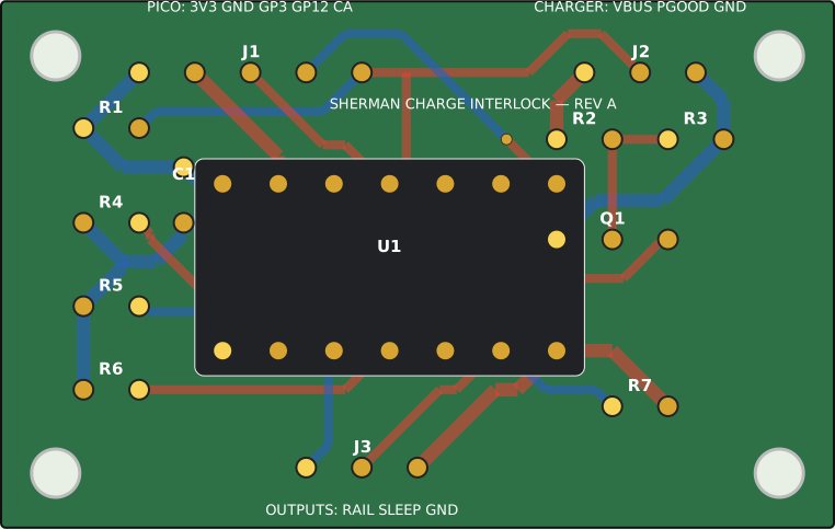
Charging interlock rev a is an open-source printed circuit board by dsorensen228, from the dsorensen228/sherman repository on GitHub. It is a 2-layer board of 38.1 × 24.1 mm with 17 parts on 9 nets, routed with 86 tracks and 3 vias.
It is built around the SN74HC08N and 2N3904BU. Its parts include 7 resistors, 3 connectors, 1 capacitor, 1 IC and 1 transistor. It belongs with the robots and motor control and computers and single-board computers boards and the RP2040 boards of this library.


This 38.10 mm × 24.13 mm two-layer through-hole board is the dedicated compact implementation of the W1 automatic, redundant charge-present motor inhibit from ADR 0004. Plugging power into the Adafruit #4755 remains the only V1 charging action.
Status: three bare boards and parts for two populated assemblies were ordered
2026-09-01. Receiving inspection and electrical qualification remain pending.
Installing the board in an unrestrained mobile Sherman is not released until the
bench truth table and power-order fault matrix in
electronics/TESTING.md pass.
The OSH Park order used
charging-interlock-rev-a-gerbers.zip
without unpacking it and the following fabrication settings. The selected
service level and final paid total remain in the vendor receipt rather than this
repository.
The submitted-order contents and receiving checklist are recorded in
order-manifest.md.
| Setting | Value |
|---|---|
| Layers | 2 |
| Size | 38.10 mm × 24.13 mm (detected from the outline) |
| Material | FR-4 |
| Thickness | 1.6 mm / 0.063 inch |
| Copper | 1 oz outer layers |
| Finish | OSH Park ENIG |
| Solder mask / legend | Vendor default; front legend required |
| Assembly | None—bare PCB only |
| Quantity | 3 bare boards ordered; at least 2 good boards required |
Populate two: one for Sherman and one complete tested spare. Keep the third bare as a fabrication spare unless receiving inspection rejects one of the first two.
The generated layout uses 0.4064 mm signal tracks, 0.6096 mm supply/ground tracks, 0.3048 mm minimum copper clearance, 0.6096 mm minimum via drill, and 0.8128 mm minimum component drill. These are deliberately conservative relative to the selected vendor's standard two-layer process.
Square copper pads are pin 1. Do not use ribbon color as identity; continuity check each completed harness endpoint.
| Connector | Pin 1 | Pin 2 | Pin 3 | Pin 4 | Pin 5 |
|---|---|---|---|---|---|
J1 PICO | Pico pin 36 3V3(OUT) | Pico pin 23 GND | Pico pin 5 GP3 | Pico pin 16 GP12 | Pico pin 9 GP6 / CHARGE_ABSENT observer |
J2 CHARGER | #4755 VBUS | #4755 PGOOD | #4755 GND | — | — |
J3 OUTPUTS | Pololu #2808-M CTRL | DRV8833 SLP/nSLEEP | driver/power-gate GND | — | — |
J1.5 is an input-only observation at the Pico. Firmware must never drive it.
J2.2 PGOOD is active-low/open-drain. Q1 supplies a second immediate inhibit
from raw VBUS.
bom.csv is the per-board BOM. The ordered and required totals are:
| Part | Needed for 2 | Ordered | Mouser # |
|---|---|---|---|
TI SN74HC08N PDIP-14 | 2 | 2 | 595-SN74HC08N |
TE 1-2199298-3 14-pin DIP socket | 2 | 2 | 571-1-2199298-3 |
onsemi 2N3904BU | 2 | 5 | 512-2N3904BU |
KEMET C315C104K5R5TA 100 nF X7R | 2 | 10 | 80-C315C104K5R5TA |
Yageo MFR-25FRF52-10K 10 kOhm 1% | 8 | 10 | 603-MFR-25FRF5210K |
Yageo MFR-25FRF52-47K 47 kOhm 1% | 2 | 10 | 603-MFR-25FRF52-47K |
Yageo MFR-25FBF52-100K 100 kOhm 1% | 2 | 10 | 603-MFR-25FBF52-100K |
Yageo MFR-25FRF52-4K7 4.7 kOhm 1% | 2 | 10 | 603-MFR-25FRF52-4K7 |
Samtec TSW-140-07-L-S 2.54 mm male header | 22 positions | 40 positions | 200-TSW14007LS |
The order covers both PCB assemblies with the stated overage. It does not cover
the four separate 10 kOhm pull-downs at the DRV8833 AIN1/AIN2/BIN1/BIN2
inputs; those come from general wiring stock. R7 on this PCB is already the
4.7 kOhm SLEEP_EN pull-down, so do not add a second one at the driver.
The resistors mount vertically at R1–R7; insulate the folded lead with
heat-shrink if it could touch the resistor body or an adjacent lead. Install the
DIP socket first, align its notch with the U1 outline/notch, and insert U1 only
after resistance and supply-short checks pass. Q1 is the exact onsemi
2N3904BU; with its flat face following the board outline, pins are E-B-C at
1-2-3.
3V3, VBUS, and
GND; verify all same-name connector/pad paths from netlist.csv.J1.1/J1.2; confirm the socket supply
pins are correct, then remove power and install U1.VIN, and motors disconnected. Perform
the Section 10 truth table in wiring-guide.md.SHERMAN and one SPARE
and record the measurements in the P3-PWR-001 evidence packet.generate.py is the editable source of truth. It deterministically
creates the KiCad board, assembly SVG, CSVs, Gerbers, drill files, job file,
verification report, and order ZIP:
python3 electronics/pcb/charging-interlock-rev-a/generate.py
python3 -m unittest electronics.tests.test_charging_interlock_pcb
The generator performs pad/track clearance and full-net connectivity checks. The order ZIP was also independently parsed as a two-copper-layer stack with top/bottom mask, front legend, profile, and separate plated/non-plated drills.
References: TI SN74HC08N, onsemi 2N3904 datasheet, and OSH Park two-layer specifications.
| Qty | Value | Footprint | References |
|---|---|---|---|
| 4 | 10k | Sherman:R_Axial_Vertical_P2.54mm | R1, R4, R5, R6 |
| 1 | 100k | Sherman:R_Axial_Vertical_P2.54mm | R3 |
| 1 | 100nF | Sherman:C_Disc_D5.0mm_W2.5mm_P2.54mm | C1 |
| 1 | 2N3904BU | Sherman:TO-92_Inline | Q1 |
| 1 | 4.7k | Sherman:R_Axial_Vertical_P2.54mm | R7 |
| 1 | 47k | Sherman:R_Axial_Vertical_P2.54mm | R2 |
| 1 | CHARGER | Sherman:PinHeader_1x03_P2.54mm_Vertical | J2 |
| 1 | OUTPUTS | Sherman:PinHeader_1x03_P2.54mm_Vertical | J3 |
| 1 | PICO | Sherman:PinHeader_1x05_P2.54mm_Vertical | J1 |
| 1 | SN74HC08N | Sherman:DIP-14_W7.62mm_Socket | U1 |
The 13 most common of 17 parts.

Telfair8632/sr71-600
Twin-engine 600 mm RC Blackbird: parametric FreeCAD CAD, a 14-level Pico 2 firmware verification ladder, and a complete QA-evidenced digital build package


sierrafoxtrot/PDP-8_Serial_AIO
A W070 compatible serial interface for the original DEC PDP-8


blkhurst/kicad-usb-c
This USB-C Powered AND Gate is the first PCB I have designed using KiCad, and serves as a proof of concept for integrating USB-C power into future projects. The design includes:


It measures 38.1 × 24.1 mm and has 2 copper layers, 1.6 mm thick.
17 parts, built around the SN74HC08N and 2N3904BU. The full list of its parts is on this page, with links to each part's symbol and footprint where PCBKit's library has them.
From the dsorensen228/sherman repository on GitHub, at the commit this page was made from: the board is electronics/pcb/charging-interlock-rev-a/charging-interlock-rev-a.kicad_pcb. PCBKit opens the board in the browser, with nothing to install.
Its repository states no licence, so its author keeps all rights: ask dsorensen228 before reusing the design.