4 layers94 × 50.8 mm
 drandyhaas/KiCadRoutingTools744
A set of Python/Rust tools to aid routing in KiCad
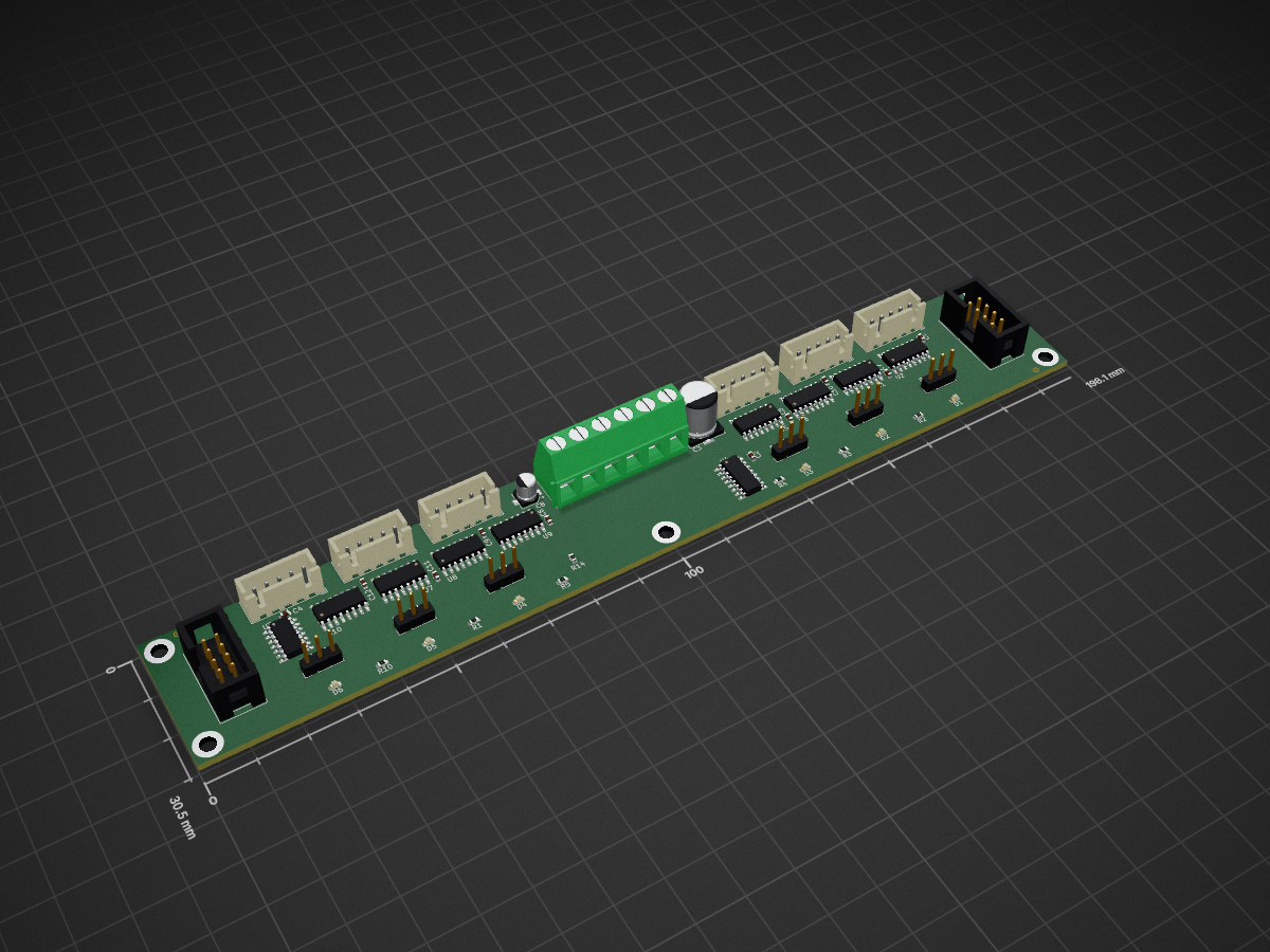
Splitflap driver is an open-source printed circuit board by drandyhaas, from the drandyhaas/KiCadRoutingTools repository on GitHub, published under the MIT licence. It is a 2-layer board of 198.1 × 30.5 mm with 65 parts on 83 nets.
It is built around the 74HC125D, TPL7407LD and 74HC595, with the 74HC165D among its other parts. Its parts include 17 connectors, 13 resistors, 12 capacitors, 10 ICs and 6 diodes.



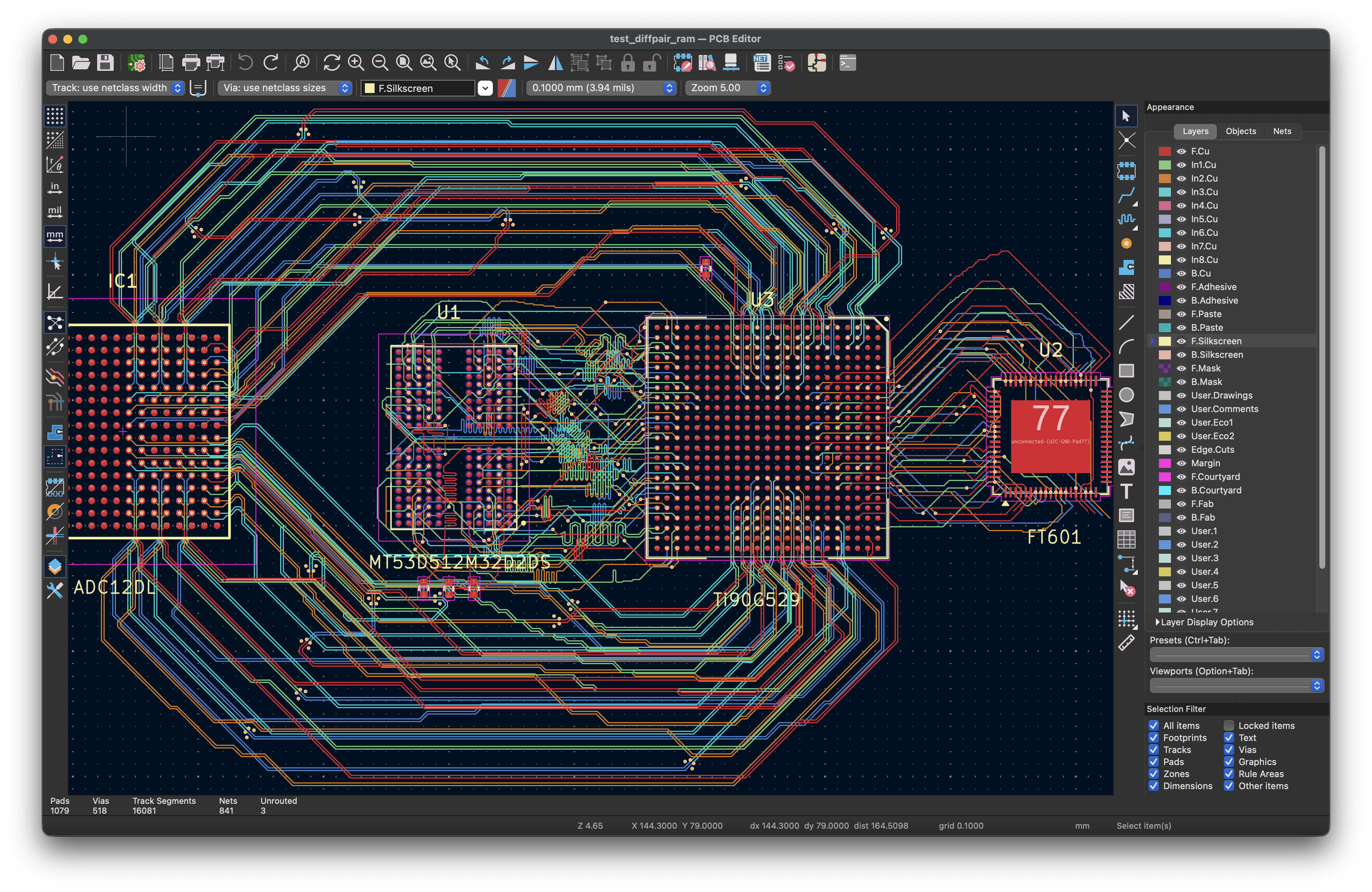
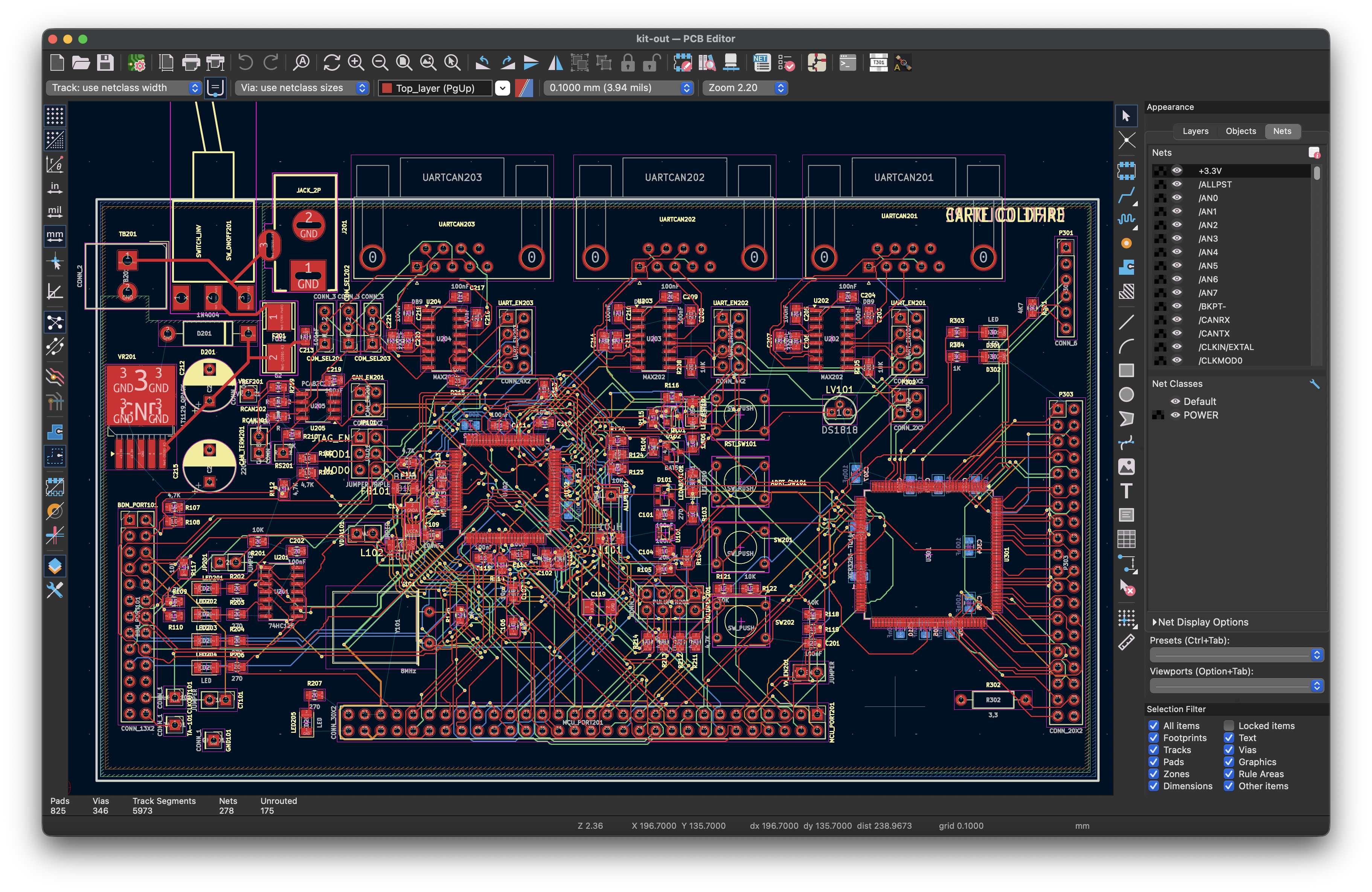
A fast Rust-accelerated A* autorouter for KiCad PCB files. Compatible with KiCad 9 and KiCad 10. Available as both a KiCad Plugin with full GUI and a Command-Line Interface for scripting and automation.
📊 Project metrics — installs, downloads and traffic, updated daily.

Free and MIT-licensed. Donations cover the ~$500/month of cloud compute and AI development behind it.
Also via GitHub Sponsors or PayPal — see Support.
--help / configuration.md)KiCadRoutingTools is free and MIT-licensed, and it stays that way — there is no paid tier, no feature held back, and nothing in this repository is paywalled.
Donations go to what it costs to build and maintain it: about $500/month of cloud computing and AI-assisted development.
The compute is not incidental. Every change to the router is A/B-tested by replaying a corpus of real open-source boards on rented cores and grading each one for DRC violations and unconnected nets, and the ~770-file test suite fans out the same way. It is what stops a change that helps one board from quietly breaking ten others.
A donation buys no priority support and unlocks no features. If you would rather contribute something worth more than money, route one of your own boards and file an issue for whatever breaks — see Contributing.
Fast, grid-based A* routing with a native Rust core (~10× faster than pure Python): octilinear (H/V/45°) multi-layer routing with automatic vias, and batch routing with incremental obstacle caching. Highlights below link to the full deep-dive docs.
Core routing
Differential pairs — see Differential Pairs
Power & planes — see Plane Routing and Power Nets
Signal integrity
Placement, fanout & optimization
place_simple.py) over 12 seeds (6 started scattered, 6 with each group gathered), and a fast route (route.py --quick 2) of the 6 the objective rates best to keep the best (/plan-pcb-placement)Cleanup & verification — see Utilities
check_weird.py), and pad geometryInterfaces
route_render.py), placement stills (render_placement.py), a board's power components (render_power.py), and movies of a routing run (route_movie.py, made for every stress run) and of a placement, or the placement skill's whole flow through to the full route (place_movie.py)make_plan.py), run it headless through the real plugin (run_plan.py), or load it in the GUI# Clone with git
git clone https://github.com/drandyhaas/KiCadRoutingTools.git
cd KiCadRoutingToolsOr download the ZIP and extract it.
Commands here use python3. On Windows, use py -3 (or python) if python3 is not found.
python3 build_router.pyBy default this downloads a prebuilt binary for your OS from the project's GitHub Releases — no Rust toolchain required. Prebuilts are published for:
If a prebuilt isn't available for your platform (e.g. Linux arm64) or the download fails, the script falls back to building locally with cargo.
If you'd rather build locally — or you're on a platform without a prebuilt — install Rust from rustup.rs:
# macOS / Linux
curl --proto '=https' --tlsv1.2 -sSf https://sh.rustup.rs | sh

# Windows: Download and run rustup-init.exe from https://rustup.rs/
After installation, restart your terminal or run source ~/.cargo/env, then:
python3 build_router.py --from-source     # build locally instead of downloading
python3 build_router.py --tag v0.15.0     # download a specific release
python3 build_router.py --clean # remove all build artifactsOption A: KiCad Plugin (Recommended for interactive use)
# Install the plugin
python3 install_plugin.py

# Then in KiCad: Tools → External Plugins → KiCadRoutingTools
Option B: Claude Code (AI-assisted routing)
Use Claude Code to analyze your PCB and generate a routing plan:
> /plan-pcb-routing kicad_files/my_board.kicad_pcbClaude will:
Other useful skills:
> /find-high-speed-nets kicad_files/my_board.kicad_pcb       # Identify high-speed nets via datasheet lookup
> /analyze-power-nets kicad_files/my_board.kicad_pcb         # Identify power nets and track widths
> /identify-diff-pairs kicad_files/my_board.kicad_pcb        # Find diff pairs by pin function, recommend gap/impedance
> /recommend-stackup kicad_files/my_board.kicad_pcb          # Stackup advice for impedance/time-matching accuracy
> /recommend-plane-mappings kicad_files/my_board.kicad_pcb   # Which nets get planes, on which layers
> /diagnose-routing-failures my_board.kicad_pcb /tmp/route_output.txt  # Root-cause failed routes, get a retry command
> /review-routed-board my_board_routed.kicad_pcb             # Post-route QA: DRC, connectivity, length match, GND vias
> /plan-pcb-placement full kicad_files/my_board.kicad_pcb    # Group, place 12 seeds, fast-route the 6 cheapest, keep the best, route end to end
See Claude Skills for what each skill does and how they fit together.
All of these are also available inside KiCad without leaving the plugin - see AI assistance in the plugin below. The plugin can run the analysis and routing skills through opencode instead of Claude Code (issue #503) - a Backend dropdown on the AI Drive tab selects the agent CLI, and opencode's provider/model strings open the door to other model providers. The placement runs need Claude Code, because they write files and opencode's analysis agent may not. The skills' output contracts are tuned on Claude models; smaller models may follow them less reliably.
Option C: Manual Command Line (For scripting and automation)
# Optionally place the board first, by its functional groups (see py_placer/placement/README.md)
python3 py_placer/place_simple.py my_board.kicad_pcb placed.kicad_pcb --groups groups.json --intent intent.json

# Pour the planes FIRST (#562): the fanout's plane-drop vias then land on
# real fill, and the route step welds plane pads into it.
python3 py_router/route_planes.py my_board.kicad_pcb poured.kicad_pcb --nets GND --plane-layers B.Cu

# Fan out a BGA, then tidy decoupling caps off the new vias (issue #130)
python3 py_router/bga_fanout.py poured.kicad_pcb -c U1 -o fanned.kicad_pcb --clearance 0.1
python3 py_placer/place_fanout_clearance.py fanned.kicad_pcb capclean.kicad_pcb --clearance 0.1

# Route differential pairs (the output is positional: route_diff's -o is --ordering)
python3 py_router/route_diff.py capclean.kicad_pcb diffed.kicad_pcb --nets "*lvds*"

# Route ALL remaining nets, plane nets included (their widths via --power-nets).
# This step ends with the in-run plane finalize that completes the planes.
python3 py_router/route.py diffed.kicad_pcb routed.kicad_pcb --nets "*" \
--power-nets GND --power-nets-widths 0.3The plugin provides a full graphical interface for all routing features, running directly within KiCad 9 or 10.
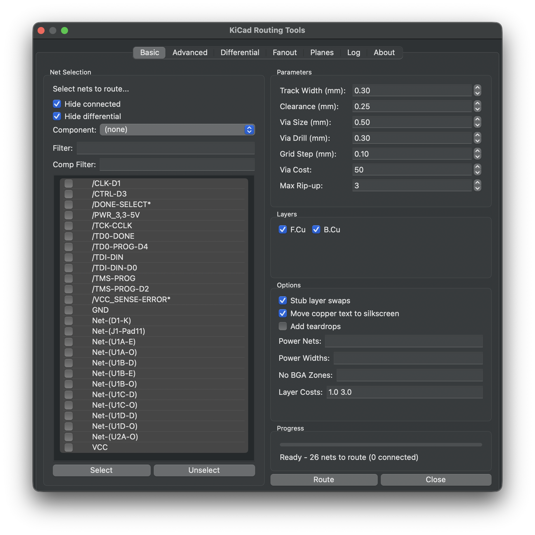
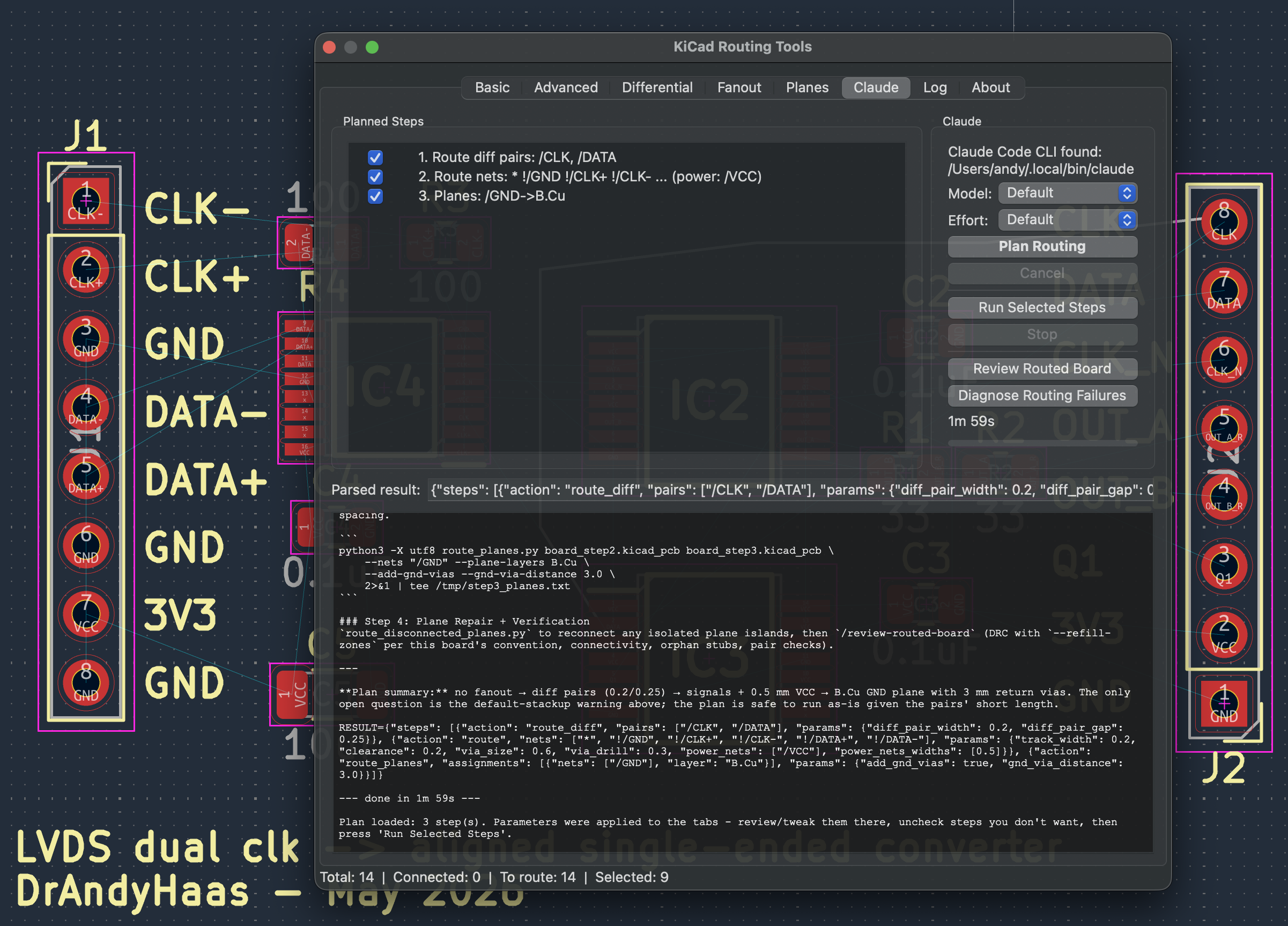
With Claude Code or opencode installed, the routing dialog gains AI assistance throughout (the plugin spawns the selected agent CLI headless, streams a live transcript, and fills GUI controls from the results). The Backend dropdown on the AI Drive tab picks the CLI: Claude Code runs Anthropic models; opencode takes provider/model strings for many providers (including its built-in free tier), with opencode auth login adding provider accounts. Both discover the same .claude/skills/; opencode runs them under a read-only pcb-analysis agent defined in opencode.json (the equivalent of the Claude run's read-only tool allowlist). Neither grants a dedicated write tool, though both grant Bash, so neither is a sandbox — the allowlist states intent, and --allowedTools auto-approves rather than restricts. Both can dispatch a subagent, so an analysis skill can hand its close-out to an independent verifier (#552): the Claude allowlist grants the dispatch tool per run, and the pcb-analysis agent grants opencode's task tool in opencode.json. A caller asking opencode for a tool set naming Write/Edit is refused rather than silently downgraded.
The tab has two sub-tabs:
/plan-pcb-routing: the plan fills the parameter fields across the tabs and appears as a checkable step list, which Run Selected Steps executes sequentially in-process on the live board with per-step status marks. Review Routed Board and Diagnose Routing Failures give post-route QA and failure root-causing. Backend, model, and effort selectors control every AI run and persist with the dialog settings (model/effort remembered per backend)./plan-pcb-placement place / full headless into a krt_placement/ folder beside the board. The tab shows the seed candidates with a preview, a status line read from the run's milestone ledger, and at the end REPORT.md; Apply Result to Board moves the open board's parts to the result's poses and locks (and, after Place + Route, its routed copper). These two need Claude Code. Beautify Labels (no AI) tidies the reference-designator silkscreen (py_placer/beautify_labels.py).python3 py_router/make_plan.py <run dir>; see Plans from the command line).The full button-to-skill map is in Claude Skills - Plugin GUI Integration. Datasheet-based skills use web lookups and take a few minutes; every run shows a live transcript with cancel.
Three ways to install:
A. KiCad Plugin and Content Manager (PCM) — the recommended path for end users, and it needs no extra repository URL: the package has been in the official KiCad repository (the one KiCad ships with, gitlab.com/kicad/addons) since v0.15.6. Open the PCM from the KiCad main window, leave the repository dropdown on KiCad official repository, go to the Plugins tab, search for routing, select KiCad Routing Tools and click Install, then Apply Changes at the bottom. If it is not listed, the PCM is serving a cached catalogue — press Refresh and look again. Versions are published with status testing rather than stable, which the PCM shows in the Status column but does not hide or block; kicad_version is a minimum, so the 9.0 entry installs on KiCad 10 as well. On first launch, the plugin checks the Python packages listed in requirements.txt (numpy, scipy, shapely, and the optional Pillow, without which only board renders and the placement preview are off) and offers a one-click pip install for any that are missing or too old into KiCad's Python. Do not assume KiCad supplies them: what it bundles varies by version and platform, and KiCad 10 on macOS ships no numpy at all. The check reports the version and the file path the running interpreter imports — KiCad's Python is often not the one pip show numpy answers for in a terminal.
B. PCM "Install from File…" using the release zip — for a release newer than the one the official catalogue currently carries, for a pinned older version, or for an offline machine. Each GitHub Release ships a ready-to-install PCM package zip named KiCadRoutingTools-<version>.zip (a single cross-platform archive bundling the prebuilt Rust binaries for all platforms — not the auto-generated "Source code (zip)"). To install it:
KiCadRoutingTools-<version>.zip (e.g. KiCadRoutingTools-0.15.13.zip).The plugin appears under Tools → External Plugins in the PCB Editor. The same first-launch scipy/shapely dependency check described in (A) applies. This path keeps the plugin manageable from the PCM (you can update or uninstall it there), unlike the manual install below.
C. Manual install from source — for development or for using the CLI tools as well:
# Install the plugin (copies to KiCad plugins directory)
python3 install_plugin.py

# For development: create symlink instead of copying
python3 install_plugin.py --symlink

# Remove the plugin
python3 install_plugin.py --uninstall

# Skip installing the Python dependencies
python3 install_plugin.py --no-deps
The installer installs into every KiCad version it finds (version directories and install roots are discovered, not taken from a fixed list), under:
~/Documents/KiCad/<version>/3rdparty/plugins/~/.local/share/kicad/<version>/3rdparty/plugins/~/Documents/KiCad/<version>/3rdparty/plugins/The installer also installs requirements.txt into KiCad's Python with pip, and skips pip when that Python already has everything. On Linux, KiCad runs the system Python, which Debian 12+, Ubuntu 23.04+, Fedora 38+ and Arch mark as externally managed (PEP 668) so pip refuses to install into it; there the installer runs no pip and prints the apt / dnf / pacman command for whatever is missing, plus the explicit --break-system-packages override for a package your distribution does not carry.
If you previously installed this plugin through the Plugin & Content Manager, that copy sits next to the local install and would shadow it on sys.path (causing stale-code errors). The installer detects any such PCM copy and moves it aside to <kicad-base>/disabled_pcm_plugins/<version>/, leaving it recoverable. Pass --keep-pcm to skip this.
The full release flow — version bump, GitHub Release, and the merge request to the official KiCad PCM repository — is documented step by step in docs/release-pipeline.md.
Short version:
VERSION and the versions[] entry in metadata.json (and rust_router/Cargo.toml only when the Rust crate changed); python3 check_release_version.py --tag vX.Y.Z checks they agree.git tag v0.15.6 && git push --tags — CI builds all 4 platform binaries, packages a single KiCadRoutingTools-<ver>.zip (the PCM validator rejects duplicate version strings, so we ship one cross-platform zip), patches metadata.json with real sha256/size values, and attaches everything to the GitHub Release.gitlab.com/kicad/addons/metadata and open an MR. See the docs page for the exact commands.To build a zip locally for testing:
python3 package_pcm.py --binary-dir ./path/to/release/artifactsRoute Tab:
--fab-tier, --escalation, --clearance-ceiling)User.1) and tick "Follow User-layer guide path" to route the selected nets along it (waypoints, avoiding obstacles, packed non-overlapping)User.2) and tick "Keep out of User-layer polygon(s)" to keep routed tracks out of those areas (hard keepout, all routed nets)Advanced options Tab:
Differential Tab:
Fanout Tab:
Planes Tab (pour creation only since #562 — plane repair runs inside every route, and the route step welds plane pads into the pour):
AI Drive Tab — see AI assistance above:
/plan-pcb-routing and run its steps; review and diagnose; save/load plans/plan-pcb-placement; Beautify LabelsLog Tab:
About Tab:
General Features:
All --nets options support fnmatch-style wildcards and exclusion patterns:
| Pattern | Description |
|---|---|
* | All nets |
*DATA* | Nets containing "DATA" |
/* | Nets starting with "/" (hierarchical) |
Net-(U1-*) | Nets matching "Net-(U1-...)" |
!GND | Exclude net named "GND" |
!*VCC* | Exclude nets containing "VCC" |
"*" "!GND" "!VCC" | All nets except GND and VCC |
Notes:
!) remove matching nets from the result# Route all nets (default) - outputs to input_routed.kicad_pcb
python3 py_router/route.py kicad_files/input.kicad_pcb
# Route all nets, overwrite input file
python3 py_router/route.py kicad_files/input.kicad_pcb --overwrite
# Route all nets to a specific output file
python3 py_router/route.py kicad_files/input.kicad_pcb kicad_files/output.kicad_pcb
# Route specific nets (using --nets option)
python3 py_router/route.py kicad_files/input.kicad_pcb kicad_files/output.kicad_pcb --nets "Net-(U2A-DATA_0)" "Net-(U2A-DATA_1)"
# Route with wildcard patterns
python3 py_router/route.py kicad_files/input.kicad_pcb kicad_files/output.kicad_pcb --nets "Net-(U2A-DATA_*)"
# Route all nets on a component (auto-excludes GND/VCC/VDD/unconnected)
python3 py_router/route.py kicad_files/input.kicad_pcb kicad_files/output.kicad_pcb --component U1
# Route specific patterns on a component (no auto-exclusion)
python3 py_router/route.py kicad_files/input.kicad_pcb kicad_files/output.kicad_pcb --nets "/DDAT*" --component U1
# Route ALL nets on a component including power (use "*" pattern)
python3 py_router/route.py kicad_files/input.kicad_pcb kicad_files/output.kicad_pcb --nets "*" --component U1
# Pour a GND zone on B.Cu (outputs to input_routed.kicad_pcb). The pour places no
# per-pad taps: the route step that follows welds the plane pads into it (#562)
python3 py_router/route_planes.py kicad_files/input.kicad_pcb --nets GND --plane-layers B.Cu

# Create GND zone, overwrite input file
python3 py_router/route_planes.py kicad_files/input.kicad_pcb --overwrite --nets GND --plane-layers B.Cu

# Create GND zone to specific output file
python3 py_router/route_planes.py kicad_files/input.kicad_pcb kicad_files/output.kicad_pcb --nets GND --plane-layers B.Cu

# Create multiple planes at once (each net paired with corresponding plane layer)
python3 py_router/route_planes.py kicad_files/input.kicad_pcb --nets GND +3.3V --plane-layers In1.Cu In2.Cu

# VCC plane; --via-size/--via-drill size this step's own vias (thermal arrays, stitching)
python3 py_router/route_planes.py kicad_files/input.kicad_pcb --nets VCC --plane-layers In2.Cu --via-size 0.5 --via-drill 0.4

# Multiple nets sharing one layer, split round spines routed on it (use | separator)
python3 py_router/route_planes.py kicad_files/input.kicad_pcb --nets GND "VA19|VA11" --plane-layers In4.Cu In5.Cu

# Dry run to see what would be placed
python3 py_router/route_planes.py kicad_files/input.kicad_pcb --nets GND --plane-layers B.Cu --dry-run
GND return vias (--add-gnd-vias) and area stitching (--stitch-vias, --stitch-edge-fence) go in a re-run of the same pour after routing, so they place around the finished signals, and a return via needs GND poured on two layers — see Plane Routing.
Since #562 you normally do not run this step. Every
route.pyrun finishes with an in-run plane finalize that applies this same engine (pad taps + region joins), the plane-copper cleanup, and a KiCad-oracle completion check — so a pours-first chain repairs its planes automatically.KICAD_PLANE_FINALIZE=0is the kill switch. The finalize runs even when the route step finds nothing else to route (#1112), so a chain should end onroute.py, never on this script. Use the standalone script below for a board routed OUTSIDE that chain (e.g. hand-edited copper); its track and via default to the board's Default net class, not to the sizes a chain routed at, so pass--track-width/--via-size/--via-drillif they differ.
After creating power planes, regions may become split by vias and traces from other nets. Use repair_planes.py to reconnect them:
# Auto-detect all zones in PCB and repair disconnected regions (outputs to input_routed.kicad_pcb)
python3 py_router/repair_planes.py kicad_files/input.kicad_pcb

# Auto-detect all zones, overwrite input
python3 py_router/repair_planes.py kicad_files/input.kicad_pcb --overwrite

# Auto-detect all zones to specific output file
python3 py_router/repair_planes.py kicad_files/input.kicad_pcb kicad_files/output.kicad_pcb

# Specific nets and layers
python3 py_router/repair_planes.py kicad_files/input.kicad_pcb --nets GND --plane-layers B.Cu

# Customize track width and clearance
python3 py_router/repair_planes.py kicad_files/input.kicad_pcb kicad_files/output.kicad_pcb \
--track-width 0.5 --clearance 0.2Placement deltas are invisible in a board file; render them instead.
# what moved, and did it help? (ghosts at the seed poses, arrows, metrics caption)
python3 py_tools/render_placement.py placed.kicad_pcb --before seed.kicad_pcb -o delta.png

# zoom to one placement block; same block names as route.py --group
python3 py_tools/render_placement.py board.kicad_pcb --list-groups --group-by sheet
python3 py_tools/render_placement.py board.kicad_pcb --zoom-group sheet:58d913ec --per-side -o out/

# everything a placement author reads, in one artifact: escape lanes, groups, and
# lock advice (which parts should NOT move) -- locks nothing, writes no board
python3 py_tools/board_brief.py board.kicad_pcb
Toggles for --borders / --labels / --ratsnest / --arrows / --ghosts;
--per-side gives F and B panels rather than one flattened projection.
The render is triage, and so are the caption's crossings / hpwl: a
placement is judged by routing it.
# Check for DRC violations. With no -c, grades at the Default net-class clearance
# the routing steps wrote into the sibling .kicad_pro (the clearance the board was
# routed to), plus the board's .kicad_dru layer rules; falls back to 0.2mm if
# there's no project. Pass -c to override.
python3 py_router/check_drc.py kicad_files/output.kicad_pcb

# Cross-check with KiCad's own DRC engine (requires KiCad; --refill-zones avoids
# bogus zone-clearance errors from stale pours - see tests/README.md for details)
kicad-cli pcb drc --refill-zones --format json -o drc.json kicad_files/output.kicad_pcb

# ...because a routed board ships zone OUTLINES with no filled_polygon, so an
# unrefilled grade reports plane opens that are not real (#910). To ship a
# board that already carries its fills, add --write-fill to the route step, or:
python3 py_tools/fill_for_delivery.py kicad_files/output.kicad_pcb -o delivered.kicad_pcb

# Check connectivity (detects unrouted nets, broken routes, and T-junctions)
python3 py_router/check_connected.py kicad_files/output.kicad_pcb

# Check connectivity for specific nets
python3 py_router/check_connected.py kicad_files/output.kicad_pcb --nets "*DATA*"

# Check connectivity for all nets on a component
python3 py_router/check_connected.py kicad_files/output.kicad_pcb --component U1
See Utilities for every checker and its options, and
python3 krt_registry.py for every runnable tool in the clone with its purpose.
Use the /analyze-power-nets skill to identify power nets and get track width recommendations:
# Ask the AI to analyze your board with datasheet lookup
/analyze-power-nets kicad_files/my_board.kicad_pcb
The skill:
--power-nets configurationsSee Power Net Analysis for detailed documentation.
Use the /find-high-speed-nets skill to identify high-speed nets and get GND return via recommendations:
# Ask the AI to analyze signal speeds with datasheet lookup
/find-high-speed-nets kicad_files/my_board.kicad_pcb
The skill:
--gnd-via-distanceThe /plan-pcb-routing skill includes a lightweight version of this analysis (net name and
footprint pattern matching only, no datasheet lookup) and automatically includes a GND return
via step when GND planes are present. Run /find-high-speed-nets first for more accurate
recommendations based on actual component specifications.
# Run full integration test (fanout + routing + checks)
python3 tests/test_fanout_and_route.py --all

# Quick mode for faster testing
python3 tests/test_fanout_and_route.py --all --quick

# The whole suite (~770 files, about 40 minutes on one machine when last measured)
python3 tests/run_all.py
See tests/README.md for detailed documentation of all test scripts.
| Document | Description |
|---|---|
| Routing Architecture | Module structure, obstacle maps, A* algorithm |
| Python API | Using the modules as a library: parser, writer, modification, config, net analysis, impedance — with runnable examples |
| Configuration | Command-line options, GridRouteConfig parameters |
| Differential Pairs | P/N pairing, polarity swaps, via handling |
| Net Ordering | MPS algorithm, inside-out ordering, strategy comparison |
| Rip-Up and Reroute | Blocking analysis, progressive N+1 escalation, reroute loop |
| Length Matching | Trombone meanders, via barrel lengths, DDR auto-grouping, time matching |
| Bus Routing | Bus detection and filter, corridor planning, middle-out ordering, corridor attraction; the topo bus step |
| Guide Corridor | User-layer guide paths, waypoints, best-effort following |
| Power/Ground Planes | Copper zones with automatic via placement |
| Utilities | Every checker (DRC, connectivity, completion, hygiene, pads), the fanout generators, placement tools, renderers, the DRC-settings fixer |
| Design Brief | Declare what the board IS -- the facts a board file cannot contain -- and compile them into the intent (<board>.design-brief.json) |
| Floorplan Intent | Declare the floorplan, grade the board against it (check_floorplan.py) |
| BGA Fanout | BGA escape routing generator |
| QFN Fanout | QFN/QFP escape routing generator |
| Rust Router | Building and using the Rust A* module |
| Power Net Analysis | Power net detection, AI analysis, track width guidelines |
| Claude Skills | All ten AI skills: placement and routing end to end, routing plans, power/high-speed/diff-pair analysis, stackup, plane mappings, failure diagnosis, board review |
| Placement | Placement by function: groups, one annealed objective, legality, the floorplan intent's grade |
| Integration Tests | Test scripts and performance benchmarks |
| Release Pipeline | How to tag a release and submit it to the KiCad PCM (maintainers) |
KiCadRoutingTools/
├── py_router/                # Routing engine + CLI entry points (~130 modules)
│   ├── route.py                  # Main CLI - single-ended routing (ends with the in-run plane finalize, #562)
│   ├── route_diff.py             # Main CLI - differential pair routing
│   ├── route_planes.py           # Main CLI - power/ground plane pours
│   ├── repair_planes.py          # Standalone utility - repair disconnected plane regions (the chain step is absorbed into route.py's finalize, #562)
│   ├── route_render.py           # PNG still of a board from its geometry
│   ├── route_movie.py            # Movie of a routing run, step by step (route_trace.py records the router's events)
│   ├── make_plan.py              # Recorded command chain -> GUI routing plan (plan.json)
│   ├── run_plan.py               # Run a GUI routing plan headless, through the real plugin dialog
│   ├── autoplan.py               # Build a routing chain from the board itself and run it, no agent
│   ├── add_rule_area.py          # Write a copper keep-out rule area onto a board
│   ├── plane_io.py               # Plane I/O utilities (zone extraction, output writing)
│   ├── plane_obstacle_builder.py # Obstacle map building for plane via placement
│   ├── plane_blocker_detection.py # Blocker detection and rip-up for plane vias
│   ├── plane_zone_geometry.py    # Voronoi cells for a shared plane layer's split
│   ├── plane_split_raster.py     # Raster finishing of a shared plane layer's split
│   ├── plane_resistance.py       # Plane resistance and current capacity calculations
│   ├── plane_region_connector.py # Detect and route between disconnected plane regions
│   ├── routing_config.py         # GridRouteConfig, GridCoord, DiffPairNet classes
│   ├── routing_defaults.py       # Default routing parameter values
│   ├── routing_state.py          # RoutingState class - tracks routing progress
│   ├── routing_common.py         # Shared utilities for route.py and route_diff.py
│ ├── obstacle_map.py # Obstacle map building functionsOne-line summaries below (all of these modules live in py_router/); the
Python API documentation has full per-module references
(signatures, dataclass fields, gotchas) with runnable examples.
| Module | Purpose |
|---|---|
route.py | CLI for single-ended routing |
route_diff.py | CLI for differential pair routing |
route_planes.py | CLI for power/ground plane pours (#562 bare pour), thermal via arrays, stitching and GND return vias |
repair_planes.py | CLI for repairing disconnected plane regions on a board routed outside the chain (route.py's in-run plane finalize runs the same engine) |
routing_config.py | Configuration classes (GridRouteConfig, GridCoord, DiffPairNet) |
routing_defaults.py | Every default routing parameter, in one place (FAB_TIER, ESCALATION, CLEARANCE, ...) |
design_rules.py | KiCad design rules resolved in KiCad's own order (#530): pad overrides, net classes, .kicad_dru rules, Board Setup minimums |
kicad_dru.py | Per-layer clearance rules from the board's .kicad_dru (#498) |
fab_tiers.py | Fab-capability floors (--fab-tier) and the escalation policy (--escalation) |
routing_state.py | RoutingState class tracking progress, results, and PCB modifications |
routing_context.py | Helper functions for building obstacles and recording success |
routing_common.py | Shared utilities for route.py and route_diff.py (BGA zones, net resolution, length matching) |
routing_utils.py | Shared utilities (build_layer_map, iter_pad_blocked_cells) |
obstacle_map.py | Obstacle map building from PCB data |
obstacle_cache.py | Net obstacle caching for incremental obstacle map builds |
obstacle_costs.py | Stub and track proximity cost calculations |
sense_branch.py | Protected Kelvin sense branches (#1279), declared by a KiCad group named sense:<REF>.<PAD> (the join pad): the member copper and its sense pads are foreign to their own net except on the join pad, so new copper joins the branch only there |
net_keepouts.py | Net-filtered copper keep-outs from the board's .kicad_dru (disallow rules on a named rule area): the regions, stamped into the obstacle map only while a net a rule binds routes, and the audit of bound-net copper the shipped board has inside one |
keep_away.py | Pairwise keep-away between net groups (#1146): the per-net band cost and the in-band report; the design brief's keep_away rules, read for the router and the placement grade alike (#1253) |
bresenham_utils.py | Bresenham line-walking utilities for grid-based segment operations |
geometry_utils.py | Shared geometry calculations (point-to-segment distance, segment intersection, UnionFind) |
routing_constants.py | Shared constants (default layer stack, power net patterns, tolerances) |
terminal_colors.py | ANSI color codes for terminal output |
| Module | Purpose |
|---|---|
diff_pair_loop.py | Main loop for routing differential pairs |
single_ended_loop.py | Main loop for routing single-ended nets |
reroute_loop.py | Processes reroute queue for failed routes |
phase3_routing.py | Phase 3 multi-point tap routing (connects remaining pads after length matching) |
diff_pair_routing.py | Differential pair A* with centerline + offset and GND vias |
diff_pair_multipoint.py | Multi-point and hybrid (coupled middle + single-ended legs) differential pairs |
single_ended_routing.py | Single-ended net A* routing |
group_routing.py | Route, preview and undo one placement block (route.py --group/--preview/--undo) |
| Module | Purpose |
|---|---|
net_ordering.py | MPS, inside-out, and original net ordering strategies |
net_queries.py | Net queries (diff pair detection, MPS ordering, power net detection, chip pad positions) |
connectivity.py | Stub endpoints, connected groups, multi-point net detection, MST edges |
bus_detection.py / bus_corridor.py | Bus groups of nets with clustered endpoints, and one planned centerline per bus (--bus) |
diff_xnet.py | AC-coupled differential pairs (XNets) through series caps (#196) |
Key functions in net_queries.py:
identify_power_nets(pcb, patterns, widths) - Pattern-based power net detection for --power-nets CLI optioncompute_mps_net_ordering(pcb, net_ids) - MPS algorithm for optimal net orderingfind_differential_pairs(pcb, patterns) - Detect P/N pairs from net names (suffix-style aware: +/- nets only pair with each other, never with _P/_N nets sharing the same base name)Key functions in py_tools/analyze_power_paths.py (used by /analyze-power-nets skill):
analyze_pcb(filepath) - Load PCB and extract components for analysisget_components_needing_analysis(components) - Get components requiring AI classificationclassify_component(components, ref, role, current_rating_ma, notes, supply_nets) - Set component classification (supply_nets names the rails of a part whose pads carry no pintype and whose nets are not rail-named)trace_power_paths(pcb, components) - Trace each load upstream (regulators entered output to input only) to the source feeding itget_power_net_recommendations(pcb, components, paths) - Get recommended track widths (a sink's rating is charged once per net; a source's rating is a limit, never a load)| Module | Purpose |
|---|---|
layer_swap_optimization.py | Upfront layer swap optimization before routing |
layer_swap_fallback.py | Try layer swap when route fails |
stub_layer_switching.py | Low-level stub layer swap utilities |
mps_layer_swap.py | MPS-aware layer swap for crossing conflicts |
polarity_swap.py | P/N polarity swap for differential pairs |
target_swap.py | Hungarian algorithm for optimal target assignment |
rip_up_reroute.py | Rip-up blocking routes and retry |
blocking_analysis.py | Analyze which nets are blocking |
length_matching.py | Length matching with trombone-style meanders |
| Module | Purpose |
|---|---|
net_rescue.py | Last-chance scoped retry of failed nets at finer parameters, then the terminal geometry escalation |
plane_pad_tap.py / plane_region_connector.py | Plane pad taps and region joins: the engine of route.py's in-run plane finalize and of repair_planes.py |
kicad_oracle.py | KiCad-oracle reconnect: routes the exact links KiCad's own connectivity reports open |
cleanup_pipeline.py | The one ordered post-route cleanup pipeline both routing fronts run |
improvement_gate.py | Never ship a board a run made worse (#600): reverts the step when connectivity regressed |
fix_kicad_drc_settings.py | Write the routed floors into the output's .kicad_pro so KiCad's DRC grades what was routed |
protected_nets.py / tool_records.py | Records later steps must honour (matched groups, routed pairs, impedance, pour promises), kept on the board and in the .kicad_pro |
| Module | Purpose |
|---|---|
kicad_parser.py | KiCad .kicad_pcb file parser (extracts stackup, footprint values, pintypes) |
kicad_writer.py | KiCad S-expression generator |
output_writer.py | Write routed output with swaps and debug geometry |
pcb_modification.py | Add/remove routes from PCB data structure |
schematic_updater.py | Update .kicad_sch files with pad swaps from routing |
impedance.py | Impedance calculations (microstrip/stripline, width from target Z) |
memory_debug.py | Memory usage statistics and debugging |
route_render.py | PNG still of a board from its geometry: the frame every picture and movie is drawn on |
route_trace.py | With KICAD_ROUTE_TRACE=1, records each track and via as the router lays, rips and restores it (<output>_routetrace.json), for route_movie.py |
route_movie.py | Movie of a routing run, step by step |
Integration test results (tests/test_fanout_and_route.py), as measured when this table was written in January 2026; the router has changed a great deal since, so read them as orders of magnitude:
| Stage | Nets | Time | Iterations |
|---|---|---|---|
| FTDI single-ended | 47/47 | 8.6s | 319K |
| LVDS diff pairs (batch 1) | 28/28 | 29.7s | 10.2M |
| LVDS diff pairs (batch 2) | 28/28 | 28.0s | 12.0M |
| DDR diff pairs | 5/5 | 0.3s | 25K |
| DDR single-ended | 51/51 | 6.2s | 565K |
Rust acceleration provided a ~10x speedup over the original pure-Python A*.
Every tool prints its full option list with --help, and docs/configuration.md is the single source of truth for the flags — defaults, guidance, and which tool each applies to. The tool-specific guides go deeper on their area:
| Tool | Purpose | Guide |
|---|---|---|
route.py | Single-ended routing | Configuration |
route_diff.py | Differential-pair routing | Differential Pairs |
route_planes.py | Power/ground plane pours, stitching, GND return vias | Plane Routing |
repair_planes.py | Plane region repair + pad taps | Plane Routing |
bga_fanout.py / qfn_fanout.py | BGA / QFN escape fanout | BGA · QFN · Utilities |
place_fanout_clearance.py | Move decoupling caps off fanout vias | Utilities |
place_simple.py | Place a board by its functional groups | Placement |
judge_seeds.py | The seed judge: the seeds judge.json names routed by one quick (level 2) chain and scored | Utilities |
board_brief.py | Assemble what a placement author needs to read, in one artifact | Utilities · Design Brief |
check_floorplan.py | Grade a board against a declared floorplan intent | Floorplan Intent |
cover_facts.py | What the board knows about a card or module over it: connector heights, card models and their undersides, standoffs on its axes, the parts under it | Floorplan Intent |
check_*.py | DRC / connectivity / hygiene / pad checks | Utilities |
check_complete.py | Is the board DONE? One fail-closed verdict over the checks | Utilities |
krt_registry.py | Every runnable tool in the clone, what it is for, and which door (placement / routing) serves it | Utilities |
route_render.py | PNG still of a board from its geometry | Utilities |
route_movie.py / place_movie.py | Movie of a routing run / of a placement, step by step | Utilities |
render_power.py | A board's power components over its rails | Utilities |
make_plan.py / run_plan.py | Build a GUI routing plan from a recorded chain / run one headless | Plans from the CLI |
autoplan.py | Route a board end to end with no agent: a plane, fanout, decap, diff-pair and route chain built from the board itself | Utilities |
# Full option list for any tool
python3 py_router/route.py --help

# A typical chain (#562 pours-first): pour, then diff pairs, then ONE route
# over ALL nets -- plane nets INCLUDED. The pour places no taps; the route
# step welds plane pads into the fill and its in-run finalize completes them,
# so do NOT exclude the plane nets here.
python3 py_router/route_planes.py board.kicad_pcb board.kicad_pcb --nets GND --plane-layers B.Cu
python3 py_router/route_diff.py board.kicad_pcb -O --nets "*_P" "*_N" --diff-pair-gap 0.15
python3 py_router/route.py board.kicad_pcb -O --nets "*" --power-nets GND --power-nets-widths 0.3
The shared option groups — geometry, power-net widths, algorithm/strategy, proximity penalties, length/time matching, post-route DRC settings, and debug layers — apply across the routing CLIs and are documented in full in Configuration.
abi3-py39 whether it is downloaded or built
from source, so building locally does not lower the floor — on 3.8 the module
compiles and then fails to load with symbol not found ... _PyCMethod_New)pip3 install "numpy>=1.22") — below 1.22 the stack fails
with errors that name neither numpy nor this tool: scipy's "A NumPy version
=1.22.4 ... is required" and
TypeError: 'numpy._DTypeMeta' object is not subscriptable
pip3 install scipy) - used for optimal target assignment and Voronoi partitioningpip3 install "shapely>=2.0") - polygon operations: multi-net plane layers, the placement courtyard readerpip3 install Pillow; 10.1+ for full-size caption fonts) - board renders and the placement preview; without it only rendering is offpip3 install -r requirements.txt installs all of the abovepython3 build_router.py --from-source); not required when using the prebuilt binary.kicad_dru rule conditioned on a rule area is honoured as a (net-filtered) disallow keep-out, and per-layer clearance rules are honoured, but an area-scoped clearance or width rule is reported as not honouredThe most valuable contribution is routing a board we haven't seen: run
/plan-pcb-routing on your own design (or any open-hardware board), grade
the result with check_drc.py + check_connected.py, and file an issue for
anything that breaks — ideally with a pointer to the board file. Fixes and
pull requests for open issues are just as welcome. See
CONTRIBUTING.md for the full guide.
MIT License
| Qty | Value | Footprint | References |
|---|---|---|---|
| 10 | 0.1uF | Capacitor_SMD:C_0603_1608Metric | C1, C2, C4, C5, C6, C7, C9, C10, C11, C12 |
| 7 | 47k | Resistor_SMD:R_0603_1608Metric | R6, R7, R8, R9, R11, R12, R14 |
| 6 | 220R | Resistor_SMD:R_0603_1608Metric | R1, R2, R3, R4, R5, R10 |
| 6 | LED | ModifiedSymbols:LED_0603_1608Metric_Silkscreen | D1, D2, D3, D4, D5, D6 |
| 6 | Motor | Connector_JST:JST_XH_B5B-XH-A_1x05_P2.50mm_Vertical | J3, J5, J6, J7, J12, J13 |
| 6 | Sensor | Connector_PinHeader_2.54mm:PinHeader_1x03_P2.54mm_Vertical | J8, J9, J10, J11, J14, J15 |
| 5 | MountingHole | MountingHole:MountingHole_3.2mm_M3_ISO7380_Pad | H1, H2, H3, H4, H5 |
| 4 | 74HC595 | ModifiedSymbols:SOIC-16_3.9x9.9mm_P1.27mm_silk | U1, U5, U7, U9 |
| 4 | TPL7407L | ModifiedSymbols:SOIC-16_3.9x9.9mm_P1.27mm_silk | U2, U6, U8, U10 |
| 3 | Power | ScrewTerminals:Generic-5.08-2P | J16, J17, J18 |
| 2 | IDC | ModifiedSymbols:IDC-Header_2x04_P2.54mm_Vertical | J19, J20 |
| 2 | MountingHole | JLCPCB:AssemblyToolingHole | H6, H7 |
| 1 | 100uF | Capacitor_SMD:CP_Elec_8x10 | C3 |
| 1 | 10uF | Capacitor_SMD:CP_Elec_4x5.3 | C8 |
| 1 | 74HC125 | ModifiedSymbols:SOIC-14_3.9x8.7mm_P1.27mm_silk | U3 |
| 1 | 74HC165 | ModifiedSymbols:SOIC-16_3.9x9.9mm_P1.27mm_silk | U4 |
It measures 198.1 × 30.5 mm and has 2 copper layers, 1.6 mm thick.
65 parts, built around the 74HC125D, TPL7407LD, 74HC595 and 74HC165D. The full list of its parts is on this page, with links to each part's symbol and footprint where PCBKit's library has them.
From the drandyhaas/KiCadRoutingTools repository on GitHub, at the commit this page was made from: the board is kicad_files/splitflap_driver.kicad_pcb. PCBKit opens the board in the browser, with nothing to install.
Its repository publishes it under the MIT licence: you may reuse it on that licence's terms (keep the author's notice, and for a copyleft licence share your changes alike).

drandyhaas/KiCadRoutingTools
A set of Python/Rust tools to aid routing in KiCad

drandyhaas/KiCadRoutingTools
A set of Python/Rust tools to aid routing in KiCad

drandyhaas/KiCadRoutingTools
A set of Python/Rust tools to aid routing in KiCad

drandyhaas/KiCadRoutingTools
A set of Python/Rust tools to aid routing in KiCad

drandyhaas/KiCadRoutingTools
A set of Python/Rust tools to aid routing in KiCad

drandyhaas/KiCadRoutingTools
A set of Python/Rust tools to aid routing in KiCad

drandyhaas/KiCadRoutingTools
A set of Python/Rust tools to aid routing in KiCad

drandyhaas/KiCadRoutingTools
A set of Python/Rust tools to aid routing in KiCad

drandyhaas/KiCadRoutingTools
A set of Python/Rust tools to aid routing in KiCad

Twistiee/rcm
A CAN-controlled relay driver for a car. 21 universal channels, each of which is simultaneously a low-side output and an input — so the same board builds as a relay controller or as a switch panel, decided in firmware…

kieraneglin/hexagon-art
A passive breakout board: two lever-terminal inputs, three JST XH outputs, all six conductors (RX bus, two spares, +12V, GND, +5V) paralleled straight across. No active components, no regulation, nothing to configure.

Stab-Rabbit-coding/Open-Secure-ESC
Governed by AGENTS.md. Build spec: ../README.md. Plan: Serenity-UAV docs/plans/2026-09-17-001-feat-tilt-controller-open-secure-esc-build-plan.md (U4).


slu4coder/Minimal-64x4-Home-Computer
My DIY TTL home computer with VGA and PS/2 and 4x the processing power of a Commodore C64 or Apple II.