2 layers47.4 × 77.4 mm

 devbotas/pcb-wires-first
A wires-first home automation controllers
Switcher is an open-source printed circuit board by devbotas, from the devbotas/pcb-wires-first repository on GitHub, published under the CERN-OHL-S-2.0 licence. It is a 2-layer board of 37.4 × 47.4 mm with 41 parts on 34 nets, routed with 188 tracks and 32 vias.
It is built around the SLG47115V and TPD4E02B04DQAR. Its parts include 7 resistors, 6 capacitors, 5 diodes, 5 connectors and 3 switches. It belongs with the home automation and IoT boards of this library.

Wireless IoT sucks.
It's unreliable and breaks all the time. There's not such thing as reliable, maintenance-free, wireless IoT.
If it runs on batteries - that's even worse.
Another problem - central IoT hubs. If those break, lose connection, decides to reboot ar whatever - my smart house immediatelly becomes non-functional.
Put the analog wires first! So that light switches continue to operate even if smart features decide to stop working.
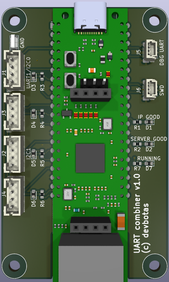
This is a simple carrier board for WizNET W55RP20 development module. It cannot do much by itself - maybe blink some LEDs. Real functionality (and also power) should come from the JST PH headers.
Can be mounted on M or L size Holey board.
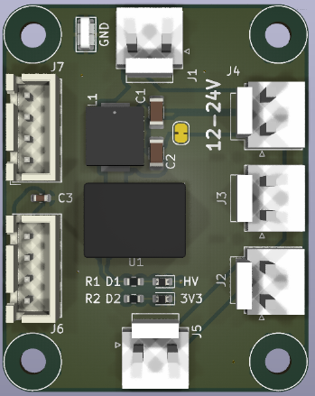
Takes 12-24V input (technically, 5-70V, but these voltages may not be supported on the other modules that this one is supposed to power) and creates 3.3V output so Gateway or other low power modules could be connected through the JST XH connector. Additionally, there are multiple JST VH connectors, which act as a power switch to connect multiple power hungry modules, like the Switcher.
Two can be mounted on a single Holey-S board.
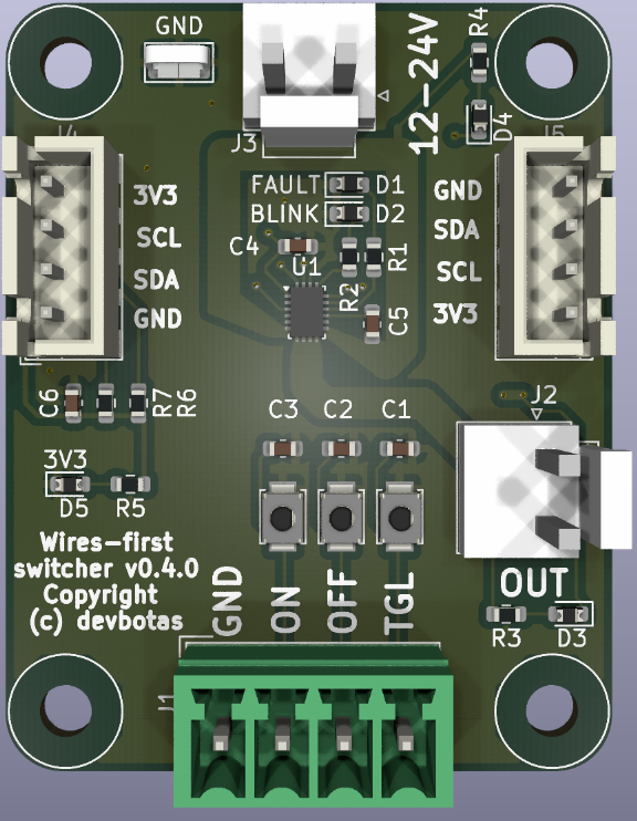
Originally meant to control LED lights, but it can switch anything. It has one switchable 12/24V output (should be able to handle 4A). Output can be controlled simultaneously in multiple ways:
The idea here that ON/OFF/TGL signals could be wired to the physical wall switches directly, any smart features being entirely optional. So the switch will operate as a dumb-switch.
Renesas HVPAK SLG47115 chip serves both as a high-power switch and an input sanitizer. For example, if faulty hardware shorts ON signal to GND permanently, OFF and TGL signals continue to operate normally.
Two can be mounted on a single Holey-S board.
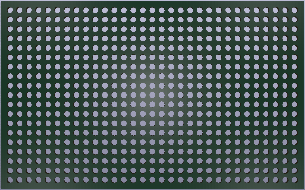
These are very handy to mount modules listed above, or maybe anything. They have a grid of 3.2mm diameter holes (hence the name) on a 5mm grid. They work perfectly with any M3 mounting hardware and come in the following sizes:
So, one M board can fit exactly two S boards, and one L board can fit exactly 2 M boards. This allows some neat and functional arrangement.
| Qty | Value | Footprint | References |
|---|---|---|---|
| 4 | 100nF | Capacitor_SMD:C_0603_1608Metric | C1, C2, C3, C4 |
| 4 | MountingHole | MountingHole:MountingHole_3.2mm_M3_NoCopper | H1, H2, H3, H4 |
| 3 | 2.2k | Resistor_SMD:R_0603_1608Metric | R1, R2, R5 |
| 3 | NetTie_2 | NetTie:NetTie-2_SMD_Pad0.5mm | NT1, NT3, NT4 |
| 3 | SolderJumper_2_Open | Jumper:SolderJumper-2_P1.3mm_Open_RoundedPad1.0x1.5mm | Bit3, PU1, PU2 |
| 2 | 4.7k | Resistor_SMD:R_0603_1608Metric | R6, R7 |
| 2 | 6.7k | Resistor_SMD:R_0603_1608Metric | R3, R4 |
| 2 | I2C | Connector_JST:JST_XH_B4B-XH-A_1x04_P2.50mm_Vertical | J4, J5 |
| 1 | 100 | Resistor_SMD:R_Array_Concave_4x0603 | RN1 |
| 1 | 1000nF | Capacitor_SMD:C_0603_1608Metric | C5 |
| 1 | 3V3 | Diode_SMD:D_0603_1608Metric | D5 |
| 1 | 4.7μF/16V | Capacitor_SMD:C_0603_1608Metric | C6 |
| 1 | BLINK | Diode_SMD:D_0603_1608Metric | D2 |
| 1 | Conn_01x02 | Connector_JST:JST_VH_B2P-VH_1x02_P3.96mm_Vertical | J3 |
| 1 | FAULT | Diode_SMD:D_0603_1608Metric | D1 |
| 1 | GND | TestPoint:TestPoint_Keystone_5019_Miniature | TP1 |
| 1 | HV | Diode_SMD:D_0603_1608Metric | D4 |
| 1 | Input | Connector_Phoenix_MC:PhoenixContact_MCV_1,5_4-G-3.5_1x04_P3.50mm_Vertical | J1 |
| 1 | NetTie_2 | NetTie:NetTie-2_THT_Pad0.3mm | NT2 |
| 1 | OUT | Connector_JST:JST_VH_B2P-VH_1x02_P3.96mm_Vertical | J2 |
| 1 | OUT | Diode_SMD:D_0603_1608Metric | D3 |
| 1 | SLG47115V | Package_DFN_QFN:Renesas_UQFN-20_2x3mm_P0.4mm_SLG47115V | U1 |
| 1 | TPD4E02B04DQA | Package_SON:USON-10_2.5x1.0mm_P0.5mm | U2 |
| 1 | reset | Button_Switch_SMD:SW_SPST_B3U-1000P | SW2 |
| 1 | set | Button_Switch_SMD:SW_SPST_B3U-1000P | SW3 |
| 1 | toggle | Button_Switch_SMD:SW_SPST_B3U-1000P | SW1 |
It measures 37.4 × 47.4 mm and has 2 copper layers, 1.6 mm thick.
41 parts, built around the SLG47115V and TPD4E02B04DQAR. The full list of its parts is on this page, with links to each part's symbol and footprint where PCBKit's library has them.
From the devbotas/pcb-wires-first repository on GitHub, at the commit this page was made from: the board is pcb/switcher/switcher.kicad_pcb and its schematic pcb/gateway/gateway.kicad_sch. PCBKit opens the board in the browser, with nothing to install.
Its repository publishes it under the CERN-OHL-S-2.0 licence: you may reuse it on that licence's terms (keep the author's notice, and for a copyleft licence share your changes alike).

devbotas/pcb-wires-first
A wires-first home automation controllers

FOSDEM/video
No longer being updated, please see the README for pointers.

NVIDIA-AI-IOT/my-jetson-nano-baseboard
An open source Jetson Nano baseboard and tools to design your own.


RoboticsBrno/Robutek
Robůtek je robotická platforma založená na čipu ESP32-S3. Je velice rozšitiřelný, ale ze základu umí jezdit, kreslit fixou, jezdit po čáře, pohybovat se bludištěm. Programování je přes Jaculus.
