

2 layers100.4 × 145.1 mm

Making my own scientific calculator!
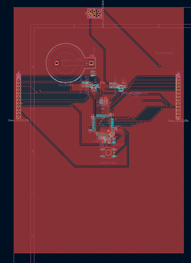
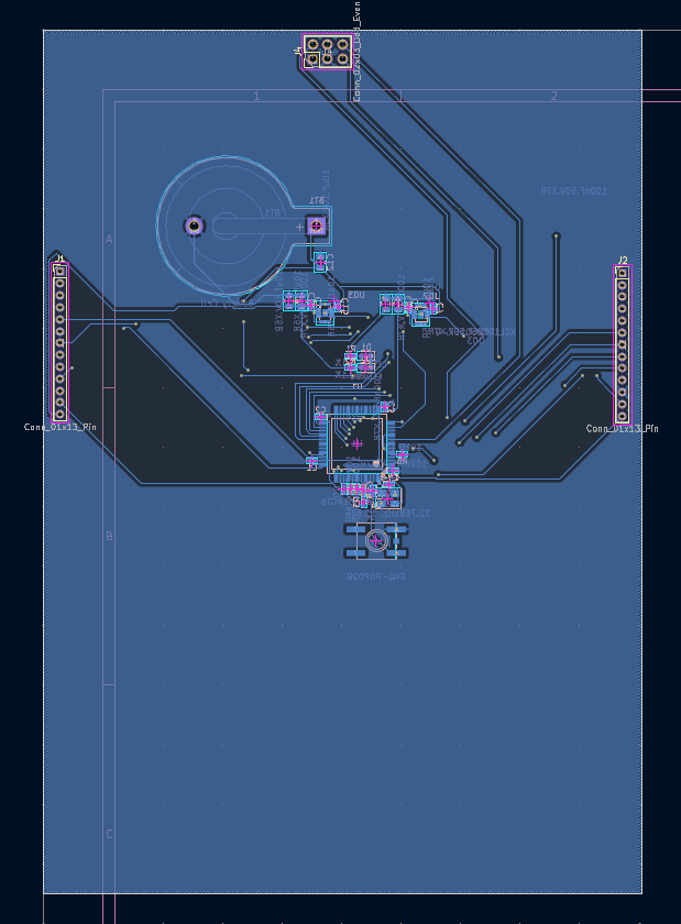
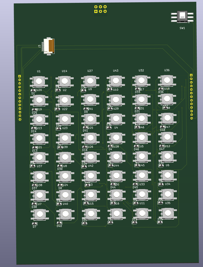
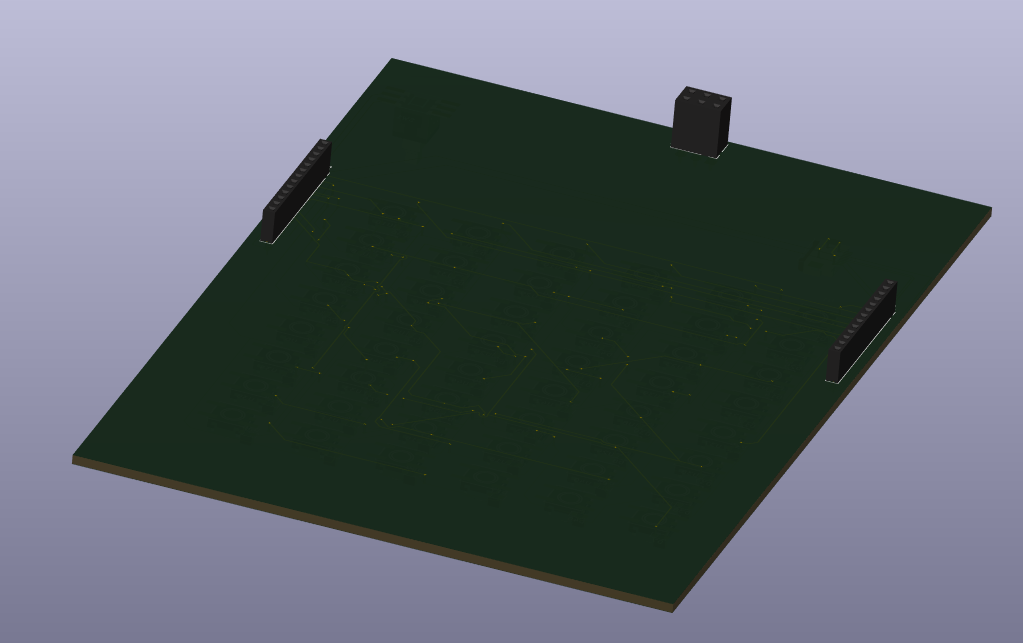
TOP is an open-source printed circuit board by damnitzhemanth-oss, from the damnitzhemanth-oss/Custom-Scientific-Calc repository on GitHub. It is a 2-layer board of 100.4 × 145.1 mm with 105 parts on 223 nets, routed with 723 tracks and 101 vias.
It is built around the EVQ-P0P02B, 1N4148W and PS-5824SVA-6PLW. Its parts include 48 ICs, 48 diodes, 3 connectors and 1 switch.
This repo mainly contains four sections,
production folders contain two CSV's, one is manual made with cost and other is KiCad Generated
Scientific calculators are just normal calculator and all other weird math symbols from trigonometry , algebra etc.
These are usually costly and bulky. So I reverse engineered and built one !.
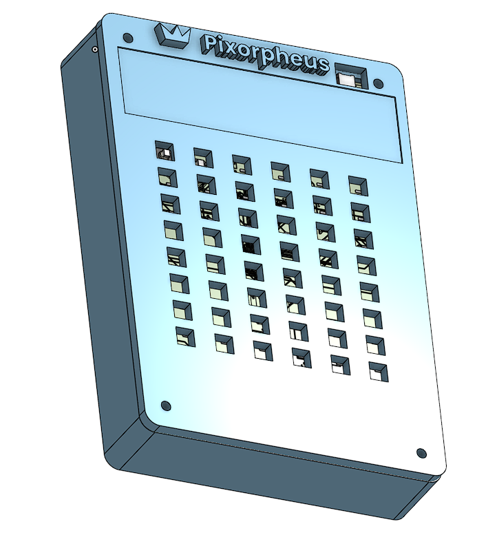
Custom-Scientific-Calc
├── CAD
│   ├── Assembly.step
│   ├── Base_Plate.step
│   └── Top_Plate.step
├── Images
│   ├── CAD
│   │   ├── Base_P_B.png
│   │   ├── Base_PlateH.png
│   │   ├── Hero_View_Final.png
│   │   ├── Top_Plate.png
│   │   └── Top_Plate_H.png
│   └── PCB
│       ├── Base
│       │   ├── PCB
│       │   │   ├── 3D.png
│       │   │   ├── 3D_B.png
│       │   │   ├── 3D_Hero.png
│       │   │   ├── B.cu.png
│       │   │   ├── F.cu.png
│       │   │   └── HeroView_PCB.png
│       │   └── Schematic
│       │       ├── Battery.png
│ │ ├── Boosters.png| # | Ref | Part / Value | Qty | Footprint | LCSC | Unit $ | Total $ |
|---|---|---|---|---|---|---|---|
| 1 | U1 | STM32L431RCT6 | 1 | LQFP-64 10x10mm | C92468 | $3.60 | $3.60 |
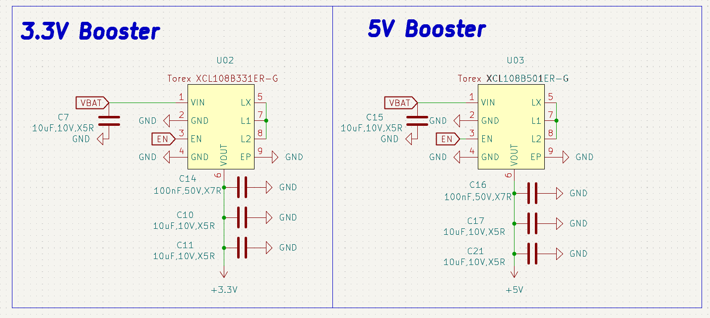
| 2 | U02 | XCL108B331ER-G (3.3V boost) | 1 | CL-2025-02 | — | $2.50 | $2.50 |
| 3 | U03 | XCL108B501ER-G (5.0V boost) | 1 | CL-2025-02 | — | $2.50 | $2.50 |
| 4 | U4 | EVQ-P0P02B (reset button) | 1 | SW-SMD_EVQ-P0P02B | C6554563 | $0.44 | $0.44 |
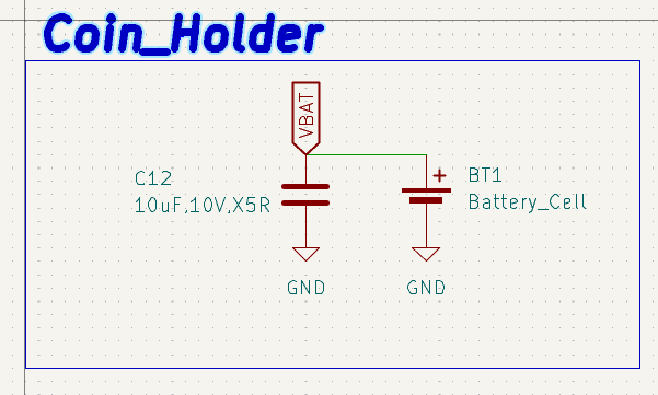
| 5 | BT1 | Keystone 103 CR2032 holder | 1 | BatteryHolder_Keystone_103 | — | $0.55 | $0.55 |
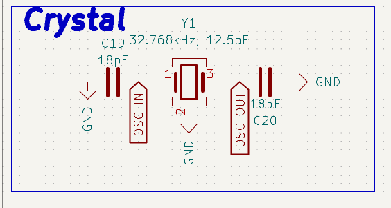
| 6 | Y1 | 32.768 kHz crystal, 12.5pF | 1 | Crystal_SMD_3225-4Pin | C32346 | $0.28 | $0.28 |
| 7 | C1–C5, C14, C16, C18 | 100nF 50V X7R | 8 | C_0402_1005 | C1525 | $0.01 | $0.08 |
| 8 | C6 | 1µF 10V X5R | 1 | C_0402_1005 | C15849 | $0.02 | $0.02 |
| 9 | C7, C15 | 10µF 10V X5R | 2 | C_0402_1005 | C19702 | $0.03 | $0.06 |
| 10 | C10, C11, C12, C17, C21 | 10µF 10V X5R | 5 | C_0805_2012 | C15850 | $0.05 | $0.25 |
| 11 | C19, C20 | 18pF 50V C0G | 2 | C_0402_1005 | C1579 | $0.01 | $0.02 |
| 12 | R1, R2 | 1kΩ 1% | 2 | R_0402_1005 | C11702 | $0.005 | $0.01 |
| 13 | R3, R8 | 10kΩ 1% | 2 | R_0402_1005 | C25744 | $0.005 | $0.01 |
| 14 | R7 | 10Ω 1% | 1 | R_0402_1005 | C103090 | $0.005 | $0.005 |
| 15 | D1 | Green LED 0603 | 1 | LED_0603_1608 | C72043 | $0.03 | $0.03 |
| 16 | D2 | Red LED 0603 | 1 | LED_0603_1608 | C2286 | $0.03 | $0.03 |
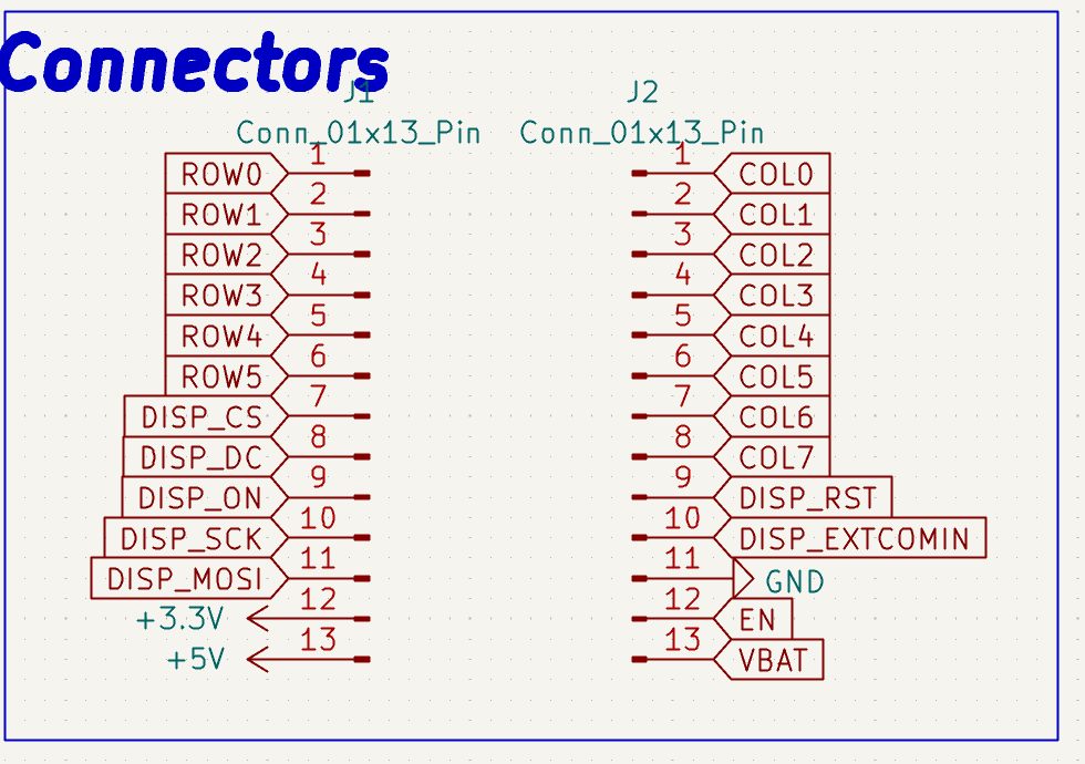
| 17 | J1, J2 | 1×13 pin header, 2.00mm | 2 | PinHeader_1x13_P2.00 | — | $0.30 | $0.60 |
| 18 | J4 | 2×3 pin header, 2.54mm (SWD) | 1 | PinHeader_2x03_P2.54 | C65104 | $0.08 | $0.08 |
BASE Subtotal: ~$11.07
| # | Ref | Part / Value | Qty | Footprint | LCSC | Unit $ | Total $ |
|---|---|---|---|---|---|---|---|
| 1 | U1–U48 | EVQ-P0P02B tactile switches | 48 | SW-SMD_EVQ-P0P02B_3d | C6554563 | $0.44 | $21.12 |
| 2 | D1–D48 | 1N4148W (anti-ghosting) | 48 | D_SOD-110 | C89641 | $0.01 | $0.48 |
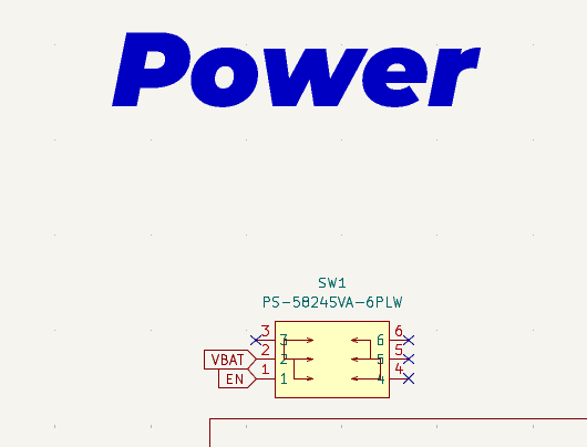
| 3 | SW1 | PS-5824SVA-6PLW (latching power switch) | 1 | SW-SMD_6P-L5.8-W5.8-P2.00 | C47018553 | $1.00 | $1.00 |
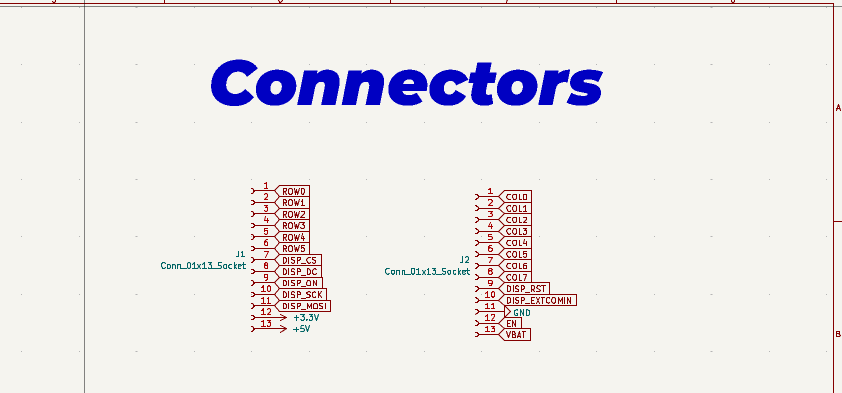
| 4 | J1, J2 | 1×13 socket, 2.00mm | 2 | PinSocket_1x13_P2.00 | — | $0.35 | $0.70 |
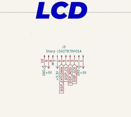
| 5 | J3 | Hirose FH12-10S-0.5SH (LCD FPC) | 1 | FFC-FPC_Hirose_FH12-10S | C506791 | $0.60 | $0.60 |
| 6 | DS1 | Sharp LS027B7DH01A 2.7" Memory LCD | 1 | external, soldered via J3 | — | $18.00 | $18.00 |
TOP Subtotal: ~$41.90
| Item | Cost |
|---|---|
| BASE PCB components | $11.07 |
| TOP PCB components | $41.90 |
| Total component cost | $52.97 |
| PCB fabrication (2 boards, 5 pcs each, JLCPCB) | ~$15.00 |
| SMT assembly setup fee | ~$8.00 |
| Extended part feeder fees (~15 parts × $1.50) | ~$22.50 |
| Stencil + labor | ~$6.50 |
| Estimated total (5 units) | ~$105 per run |
| Per unit (5 units) | ~$21 + shipping |
Torex boosters footprint was not available on internet so I created symbol and footprint.
Onshape Link : https://cad.onshape.com/documents/ad7319a20d75441a919925a9/w/2019cd65cfda231ca2b84125/e/7e9bc9015b0e0043ba3c4c11
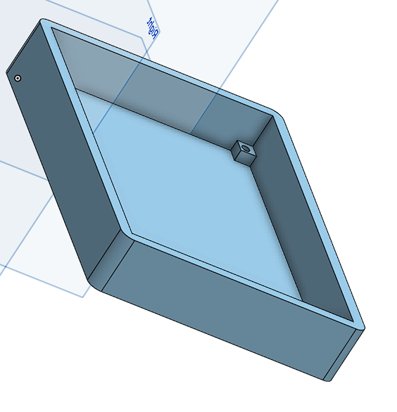
How assembly works: Base PCB and top PCB latches onto each other and gets sandwiched between Top_Plate and Base_Plate preferably with 16mm screws.
I used two torex boosters to boost 3v from Coin Cell into 5V for LCD and 3.3V for other components.
And matrix connection was used for 48 switches.
This is a test firmware. Not yet tested yet. Available as single file or 6 files (easier for debugging).
AI was used for help of Firmware and debugging problems with OnShape.
View more images in images folder
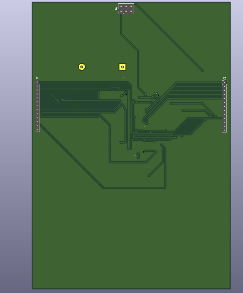
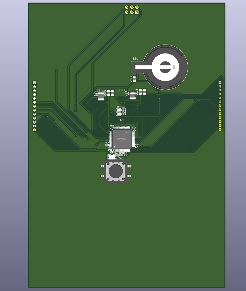
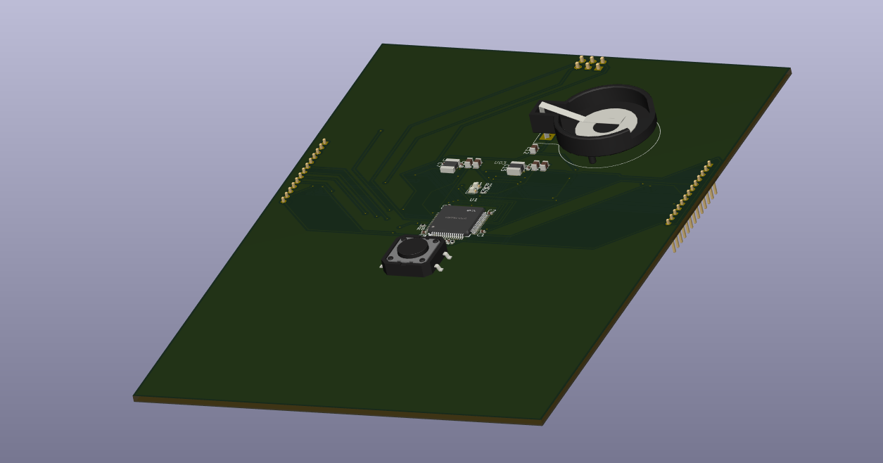
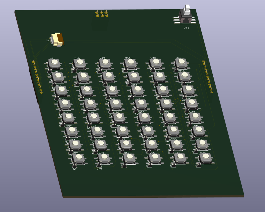
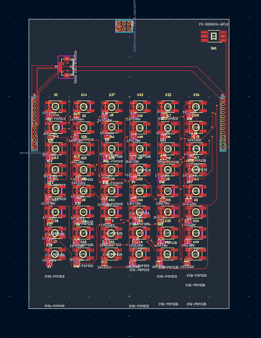
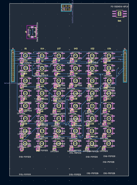
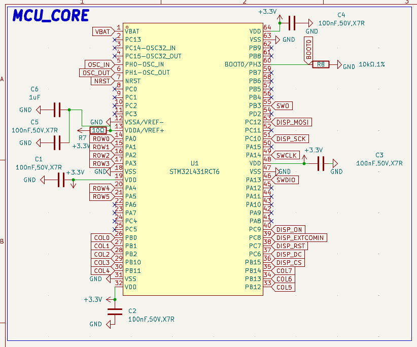
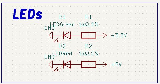
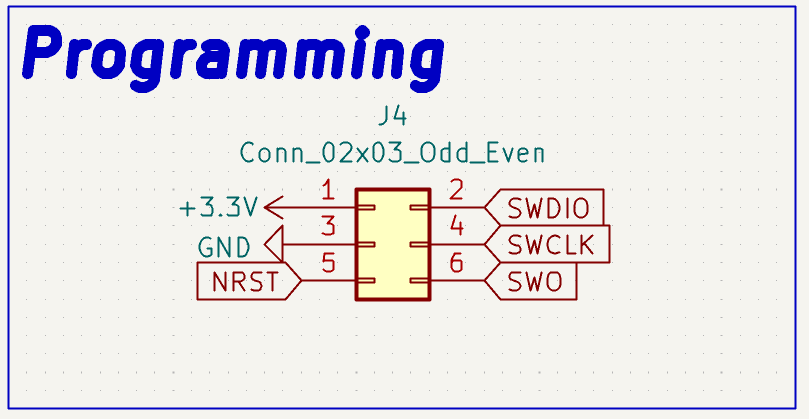
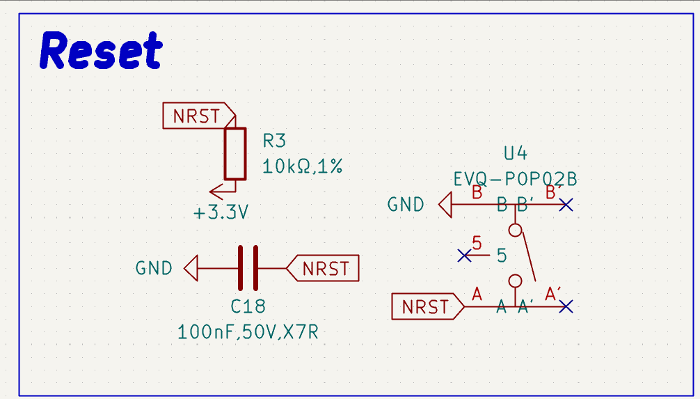
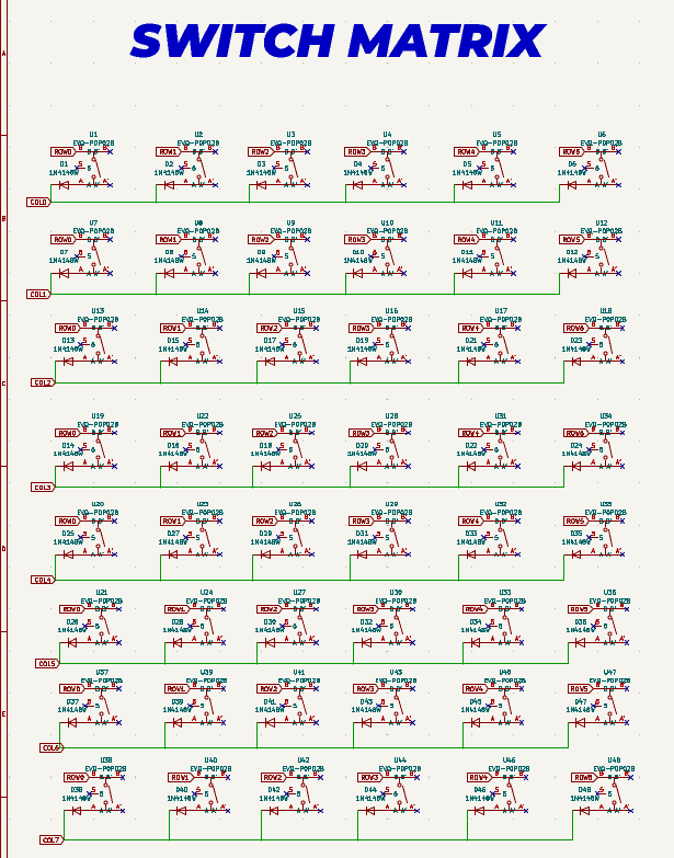
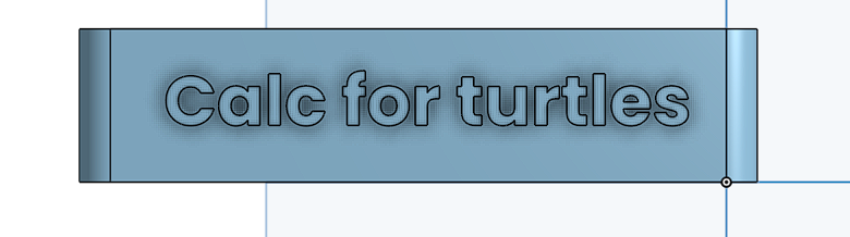
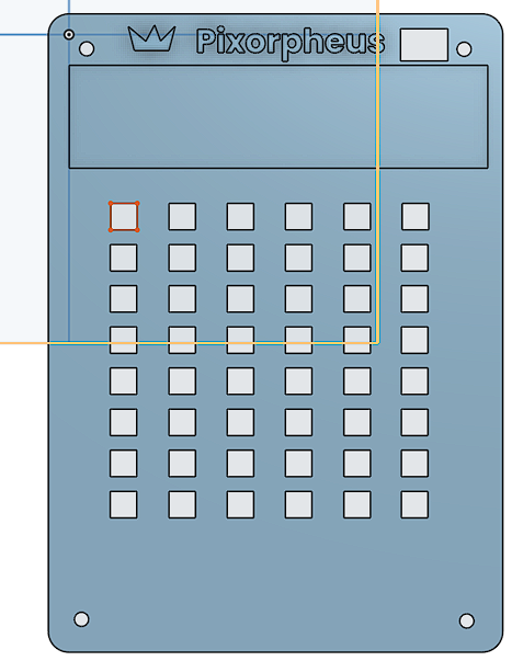
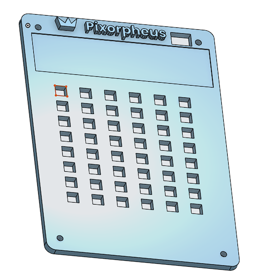
MIT License, freedom to use any of the files in the repo. But credit is appreciated!
| Qty | Value | Footprint | References |
|---|---|---|---|
| 48 | 1N4148W | Diode_SMD:D_SOD-110 | D1, D2, D10, D11, D12, D13, D14, D15, D16, D17, D18, D19, D20, D21, D22, D23 +32 |
| 48 | EVQ-P0P02B | Custom_Footprints:SW-SMD_EVQ-P0P02B_3d | U1, U2, U10, U11, U12, U13, U14, U15, U16, U17, U18, U19, U20, U21, U22, U23 +32 |
| 2 | Conn_01x13_Socket | Connector_PinSocket_2.00mm:PinSocket_1x13_P2.00mm_Vertical | J1, J2 |
| 1 | PS-5824SVA-6PLW | Custom_Footprints:SW-SMD_6P-L5.8-W5.8-P2.00-LS11.3 | SW1 |
| 1 | Sharp LS027B7DH01A | Connector_FFC-FPC:Hirose_FH12-10S-0.5SH_1x10-1MP_P0.50mm_Horizontal | J3 |
The 100 most common of 105 parts.

fossasia/pslab-hardware
PSLab Hardware Design and Schematics https://pslab.io

pierrechevalier83/ferris
A low profile split keyboard designed to satisfy one single use case elegantly


MickiusMousius/Rolio46Keyboard
A split wireless keyboard based on the Corne and Sofle


sadekbaroudi/bgkeeb
This is a reversible 100mm x 100mm pcb with support for mx or choc switches (no hotswap), per key led, rotary encoders, and exposes the SDA/SCL/GND/VCC lines in the form of the pimoroni trackball pins (meaning you can…

It measures 100.4 × 145.1 mm and has 2 copper layers, 1.6 mm thick.
105 parts, built around the EVQ-P0P02B, 1N4148W and PS-5824SVA-6PLW. The full list of its parts is on this page, with links to each part's symbol and footprint where PCBKit's library has them.
From the damnitzhemanth-oss/Custom-Scientific-Calc repository on GitHub, at the commit this page was made from: the board is PCB/Top_PCB/Project_Files/TOP.kicad_pcb and its schematic PCB/Base_PCB/Project_Files/BASE.kicad_sch. PCBKit opens the board in the browser, with nothing to install.
Its repository states no licence, so its author keeps all rights: ask damnitzhemanth-oss before reusing the design.