
2 layers88.9 × 88.9 mm

A homebrew SBC based on the WDC 65C02S and 65C22S
Pinky-8 is an open-source printed circuit board by contrarian-computing, from the contrarian-computing/pinky-8 repository on GitHub, published under the MIT licence. It is a 2-layer board of 88.9 × 71.1 mm with 37 parts on 76 nets, routed with 647 tracks and 48 vias.
It is built around the DS1813-5+ and 74AC00. Its parts include 12 connectors, 3 resistors, 2 ICs, 1 capacitor and 1 crystal. It belongs with the computers and single-board computers boards of this library.
An affordable, 6502-based SBC for education and retrocomputing that you can build yourself
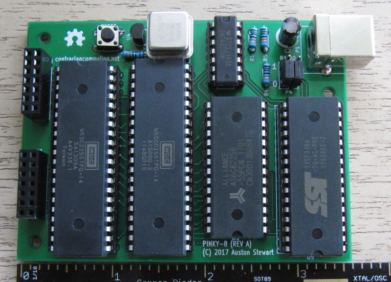 Note: The image above is of the earlier Revision A board. Revision B has similar dimensions, additional buttons and jumpers, and an improved layout permitting typical corner mounting holes.
When ARM is too much, try PINKY.
Note: The following refers to the Rev B board tag.
PINKY-8 is intended as an affordable educational and/or hobbyist device for those wishing to gain firsthand experience with the historically significant 6502 processor and vintage computer construction. As such, PINKY-8 incorporates chips still in production today that are similar to those found in commercial designs of the late 1970s and early 1980s. Building a PINKY-8 does not require scavenging parts from vintage machines and every bit can easily be soldered by hand.
PINKY-8 is a barebones SBC with onboard I/O limited to the 2 x 8-bit bi-directional GPIO pins and control lines offered by the 65C22S Versatile Interface Adapter. These are exposed in two 2x7 socket headers into which expansion boards supporting other forms of I/O (e.g. SPI, I2C, video, sound) can be plugged, similar to Arduino shields. There is no elaborate programmable bank switching for RAM or ROM, just jumpers on the board. In lieu of power regulation circuitry, PINKY-8 depends on a well-regulated 5V supply (such as a phone charger) attached via a standard USB A-to-B cable.
PINKY-8 is open-source hardware created with open-source hardware, specifically KiCad 4.0.6. Source for its ROM is located in a separate repository and can be assembled with the open-source CC65 suite.
For good performance at minimal cost, address decoding is performed using a single 74AC00 Quad NAND Gate using a scheme advanced by 6502 afficionado, Garth Wilson.
SRAM: $0000-$7FFF (32K)
VIA: $8000-$800F
ROM: $C000-$FFFF (16K)
Components have been selected to support a maximum clock speed of about 5Mhz. Beyond that faster ROM and RAM are necessary which will considerably increase the cost of a complete board. To approach the W65C02S's 14Mhz maximum rated speed requires very fast RAM into which program data is typically copied from slower ROM at boot by means of still more componentry.
The board has standard-width traces and drill holes on a two-sided design to facilitate affordable manufacturing by nearly any boardhouse.
1 x W65C02S, PDIP-40
1 x W65C22S, PDIP-40
1 x SST39SF010A-70, PDIP-32
1 x AS6C62256-55PCN, PDIP-28
1 x SN74AC00N, PDIP-14
1 x 1-5Mhz 50% Duty Cycle, 10ns Rise Time Oscillator, DIP-8
2 x DS1813-5+ (5% Tolerance), TO-92-3 w/Bent Legs
2 x Tactile Switch 6.0x6.0x4.3mm, Through Hole, 4 Lead
1 x USB B Female Through-Hole Receptacle
6 x 0.1uF 50V MLCC Axial Capacitors
3 x 3.3kOhm 1/4W Axial Metal Film Resistors
1 x 100uF 10V Radial Aluminum Electrolytic Capacitor
3 x 1x3 Pin Header .1" spacing
2 x 2x7 Female Socket Header .1" spacing (can substitute with pin header)
3 x 2-pin Jumper / Shunt, .1" spacing
2 x DIP-40 Dual wipe or machined sockets
1 x DIP-32 Dual wipe or machined socket
1 x DIP-28 Dual wipe or machined socket
1 x DIP-14 Dual wipe or machined socket
1 x DIP-8 Dual wipe or machined socket
4 x M2.5 standoffs for mounting
Detailed instructions for board assembly will be added to the wiki in time.
| Qty | Value | Footprint | References |
|---|---|---|---|
| 12 | CONN_01X01 | Wire_Pads:SolderWirePad_single_0-8mmDrill | P1, P2, P3, P4, P5, P6, P10, P11, P13, P14, P15, P17 |
| 3 | 3.3K | Resistors_THT:R_Axial_DIN0204_L3.6mm_D1.6mm_P7.62mm_Horizontal | R1, R2, R3 |
| 3 | CONN_01X03 | Pin_Headers:Pin_Header_Straight_1x03_Pitch2.54mm | B0, B1, B2 |
| 2 | DS1813 | TO_SOT_Packages_THT:TO-92_Inline_Wide | U6, U7 |
| 2 | SW_Push_Dual | Buttons_Switches_THT:SW_TH_Tactile_Omron_B3F-10xx | NMI, RESET |
| 1 | 100uF | Capacitors_THT:CP_Radial_D6.3mm_P2.50mm | C7 |
| 1 | 74AC00 | Housings_DIP:DIP-14_W7.62mm_LongPads | 74AC00 |
| 1 | AS6C62256 | Housings_DIP:DIP-28_W15.24mm_LongPads | 62256 |
| 1 | GLS29EE010 | Housings_DIP:DIP-32_W15.24mm_Socket_LongPads | 39SF010 |
| 1 | MXO45 | Housings_DIP:DIP-8_W7.62mm_Socket_LongPads | X1 |
| 1 | OSHW-logo_silkscreen-front_8mm | OSHW-logo:OSHW-logo_silkscreen-front_8mm | G*** |
| 1 | PERIPHERAL A | Socket_Strips:Socket_Strip_Straight_2x07_Pitch2.54mm | PA |
| 1 | PERIPHERAL B | Socket_Strips:Socket_Strip_Straight_2x07_Pitch2.54mm | PB |
| 1 | USB_B | Connectors:USB_B | USB-B |
| 1 | W65C02S | Housings_DIP:DIP-40_W15.24mm_LongPads | 65C02 |
| 1 | W65C22S | Housings_DIP:DIP-40_W15.24mm_LongPads | 65C22 |
The 33 most common of 37 parts.
It measures 88.9 × 71.1 mm and has 2 copper layers, 1.6 mm thick.
37 parts, built around the DS1813-5+ and 74AC00. The full list of its parts is on this page, with links to each part's symbol and footprint where PCBKit's library has them.
From the contrarian-computing/pinky-8 repository on GitHub, at the commit this page was made from: the board is pinky-8.kicad_pcb. PCBKit opens the board in the browser, with nothing to install.
Its repository publishes it under the MIT licence: you may reuse it on that licence's terms (keep the author's notice, and for a copyleft licence share your changes alike).

c0pperdragon/BreadBin
A CPU made of 7400 logic on breadboards - inside a bread bin ;-)


dbuchwald/Z80DevBoard
Simple Z80 based prototyping and development board designed as extension to Arduino Mega 2560


fran150/clementina-hardware
KiCad schematic for Clementina, a 3.3V W65C02S computer with a Raspberry Pi Pico 2 W (MIA) handling video, audio, storage and I/O.

