2 layers52.1 × 66 mm

 c0pperdragon/ByteMachine20
A generic main board to build 8-bit computers
ByteMachine is an open-source printed circuit board by c0pperdragon, from the c0pperdragon/ByteMachine repository on GitHub. It is a 2-layer board of 88.9 × 88.9 mm with 46 parts on 81 nets, routed with 793 tracks and 47 vias.
It is built around the 74HC245D, 74AC00 and 74AC32PC, with the 74HC04D, 74HC574D and NE555 among its other parts. Its parts include 12 capacitors, 9 diodes, 8 ICs, 4 resistors and 1 switch. It belongs with the retro computing and games boards of this library.


Building an 8-bit computer is not exactly trivial. There are always many components involved which are normally connected to some common address and data bus with complex control signal timings for RAM, ROM and IO controller parts and whatnot.
One common way for a hobbyist user to actually build such a contraption is using a pre-engineered PCB on which to solder all necessary parts. While this can be great fun in itself, it does not teach you much about the hardware beyond basic soldering skills.
Another way is creating the whole computer totally on breadboards. There are great resources and instructions available for this and it may actually give you the best learning experience. On the other hand, creating a huge breadboard circuit comes with its own troubles. The cables will often become a total mess, you easily disturb the wrong wires while changing anything, some wires may make bad contact and you may not get the machine to run at a higher system clock.
With this design as a building block, I wanted to provide some kind of middle ground. The PCB provides the circuity for the system bus, RAM, ROM, clock, powerup reset and rudimentary IO. You then need to add a relatively small circuit for the CPU board, depending on the type of CPU to use. This can be easily done with a single breadboard and a series of jumper links connecting this with the main board. In my experients this creates a pretty reliable setup which is even able to use clock frequencies of up to 16Mhz (for the 65Cxx types of CPUs). Currently I have built and tested setups for the following CPUs:
User oe7twj has provided me with all documention for this own setup:
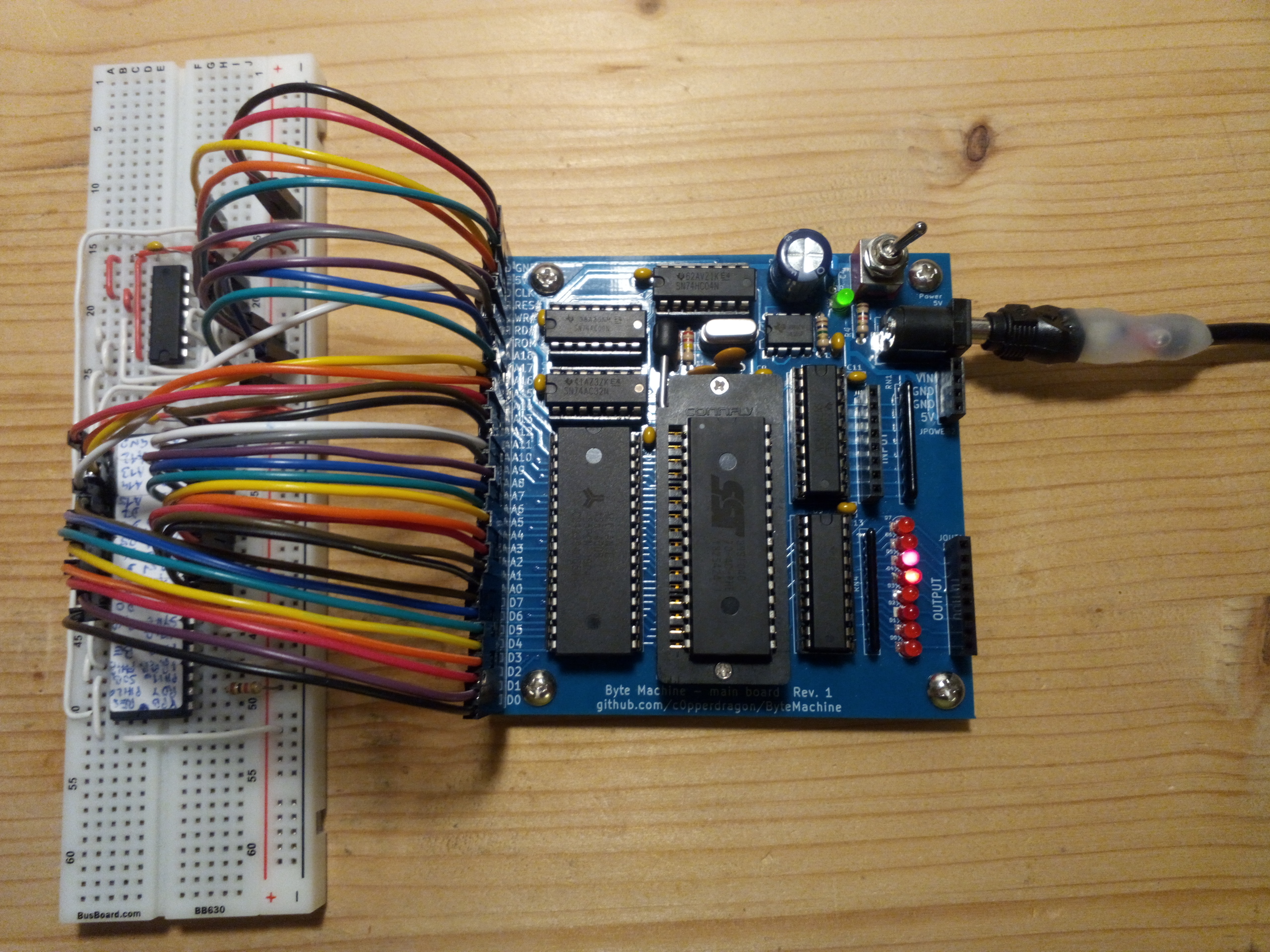
The main board has a 34 pin single-row connector that carries power and all signals necessary for the CPU to send and receive:
The main board provides a simple circuit to create a clock signal using a quartz crystal. The quartz itself is socketed, so you can easily exchange it to experiment with different frequencies. In my tests, this circuit runs reliably with frequencies from 8Mhz up to 20Mhz (but this may be too fast for your CPU).
Most (probably all) supported CPUs need some external help to cleanly start upon power-up. The power-up reset line provides a low level signal for the first few milliseconds after power is available.
Beyond providing the CPU clock, the main board itself does not use this clock for anything itself, and all accesses to both RAM, ROM and IO are triggered by asynchronous signals.
When the CPU needs to do a read, it sets up the address lines as well as the ROM selector and then pulls the RD line low. As long as this is in its low state, the board will provide the requested data on the data bus. It is in the responsibility of the CPU to never drive the data bus itself as long as the RD line is low.
For writing data to the board, the CPU needs to provide both the address (and ROM selector) and the data on the data bus. Then it needs to pull WR low and set it high again (after some minimum setup-time). The data that is present at the rising edge will be written to the RAM (or IO).
The main board contains 512K of RAM, 512K of ROM (actually a NAND-Flash IC in a ZIF socket for ease of re-programming) and two 74-series logic ICs to drive the input and output interface.
Contrary to most 8-bit computer designs, there is no dedicated address space to access IO (memory mapped IO) as this would require some complex address decoding logic. Also a dedicated IO space would reduce the address space available, and for a CPU with only 16 address lines total, this is a serious drawback.
In my solution, the only IO the CPU can do is to write into an 8-bit output port register and to read 8 bits from an input port. Writing to the output is simply done by writing anywhere to the ROM address range. The data byte written will be stored in the output register and will show up as voltages on the output port and will also directly drive the output LEDs. To also allow input with as little logic parts as possible, I chose the following mechanism: After a write to the ROM area (and in consequence to the output port as well), the main board switches to "IO mode". In IO mode, all reads from the RAM area will instead read data form the input port. To switch back to normal mode, the CPU needs to do a write to any RAM address. Using this scheme, the full range of ROM and RAM is available, as well as 8 output lines and 8 input lines.
With a total of 8 output lines and 8 input lines (each with 10K pullups), basically any kind of serial IO protocol can be implemented by the CPU: SPI, I2C, UART.
To keep things simple, the ByteBoard does not directly support any kind of IO interrupt line. Therefore basically only IO schemes are possible where the CPU is the master of the timing. This is already an inherent characteristic of the I2C and SPI bus. To implement reliable UART communication, the connected device must support hardware flow control (RTS/CTS) at least on the incomming signal, so the CPU needs only to listen for data when it is itself prepared for that.
To form the bi-directional line that is needed for I2C, one output and one input line can be combined. The output pin can for example drive an open-collector circuit (an IC or only a simple transistor circuit). An even simpler possibility is just a diode that pulls down the line when the output pin is driven low, but lets the line float when the pin is driven high. Due to the pullup resitors already present at the input port pins, this is basically all that is needed.
From the perspective of the ByteMachine, its ROM is truly read-only. So you need an external programming device to get new content onto the NAND-Flash. I am using an TL866II+ device which works absolutely fine for me. But any other compatible programmer will work, and you can even create an Arduino-Based circuit for that.
| Qty | Value | Footprint | References |
|---|---|---|---|
| 9 | LED_Small | LED_THT:LED_D3.0mm | D0, D1, D2, D3, D4, D5, D6, D7, D9 |
| 8 | 100nF | Capacitor_THT:C_Disc_D3.8mm_W2.6mm_P2.50mm | C1, C6, C7, C8, C9, C10, C11, C13 |
| 2 | 33pF | Capacitor_THT:C_Disc_D5.0mm_W2.5mm_P5.00mm | C3, C5 |
| 2 | Conn_01x08_Male | Connector_PinHeader_2.54mm:PinHeader_1x08_P2.54mm_Vertical | JIN1, JOUT1 |
| 1 | 10k | Resistor_THT:R_Array_SIP9 | RN1 |
| 1 | 10uF | Capacitor_THT:C_Disc_D5.0mm_W2.5mm_P5.00mm | C4 |
| 1 | 1M | Resistor_THT:R_Axial_DIN0207_L6.3mm_D2.5mm_P7.62mm_Horizontal | R3 |
| 1 | 1k | Resistor_THT:R_Axial_DIN0207_L6.3mm_D2.5mm_P7.62mm_Horizontal | R4 |
| 1 | 1k | Resistor_THT:R_Array_SIP9 | RN4 |
| 1 | 22 | Resistor_THT:R_Axial_DIN0207_L6.3mm_D2.5mm_P7.62mm_Horizontal | R2 |
| 1 | 220k | Resistor_THT:R_Axial_DIN0207_L6.3mm_D2.5mm_P7.62mm_Horizontal | R1 |
| 1 | 470uF | Capacitor_THT:CP_Radial_D8.0mm_P5.00mm | C2 |
| 1 | 74AC00 | Package_DIP:DIP-14_W7.62mm_Socket | U4 |
| 1 | 74AC32 | Package_DIP:DIP-14_W7.62mm_Socket | U3 |
| 1 | 74HC04 | Package_DIP:DIP-14_W7.62mm_Socket | U1 |
| 1 | 74HC245 | Package_DIP:DIP-20_W7.62mm_Socket | U7 |
| 1 | 74HC574 | Package_DIP:DIP-20_W7.62mm_Socket | U9 |
| 1 | AS6C4008 | Package_DIP:DIP-32_W15.24mm_Socket | U2 |
| 1 | Barrel_Jack_Switch | Connector_BarrelJack:BarrelJack_Horizontal | JPOWER1 |
| 1 | Conn_01x04_Male | Connector_PinHeader_2.54mm:PinHeader_1x04_P2.54mm_Vertical | JPOWER2 |
| 1 | Conn_01x34_Female | Connector_PinSocket_2.54mm:PinSocket_1x34_P2.54mm_Vertical | JBUS1 |
| 1 | Crystal | Crystal:Crystal_HC18-U_Vertical | Y1 |
| 1 | NE555 | Package_DIP:DIP-8_W7.62mm | U6 |
| 1 | SST39SF040 | ProjectFootprints:DIP-32_LargeHoles | U5 |
| 1 | SW_DPDT_x2 | ProjectFootprints:DPDS Switch | SW1 |
The 42 most common of 46 parts.
It measures 88.9 × 88.9 mm and has 2 copper layers, 1.6 mm thick.
46 parts, built around the 74HC245D, 74AC00, 74AC32PC and 74HC04D. The full list of its parts is on this page, with links to each part's symbol and footprint where PCBKit's library has them.
From the c0pperdragon/ByteMachine repository on GitHub, at the commit this page was made from: the board is mainboard/mainboard.kicad_pcb. PCBKit opens the board in the browser, with nothing to install.
Its repository states no licence, so its author keeps all rights: ask c0pperdragon before reusing the design.


c0pperdragon/BreadBin
A CPU made of 7400 logic on breadboards - inside a bread bin ;-)


slu4coder/Minimal-64-Home-Computer
Legacy: Full TTL-only home computer with VGA and PS/2 and twice the processing power of a Commodore 64


Trilobyte-CPU/8-bit-computer
A DIY 8-bit computer built mostly with discrete logic chips


rjw57/simplest-80s-computer
This is my rough scratch repo where I keep experiments to do with desiging 80s computer peripherals. It is not in any sensible shape to be used by others yet, apologies.
